In the field of 3D nano printing, how to achieve large-scale, high-quality, and continuous production has always been a core problem restricting the industrialization of the technology. Although traditional two-photon lithography (TPL) technology can achieve three-dimensional structure manufacturing with nanoscale precision, its “stop-and-go” intermittent production mode, high equipment costs, and obvious stitching defects have severely limited the commercial application of this technology.
Recently, the latest research published by Professor Shih-Chi Chen’s team at The Chinese University of Hong Kong on the arXiv preprint platform proposed a revolutionary solution – line-scanning temporal focusing two-photon lithography technology (Line-TF TPL), bringing breakthrough progress to the industrial application of 3D nano printing.
The Industrialization Dilemma of Two-Photon Lithography
Speed bottleneck: The manufacturing rate of traditional point-scanning mode is less than 10⁶ voxels per second (approximately 0.1 mm³/hour), making it difficult to meet industrial production demands. Although various parallel exposure strategies have emerged in recent years, such as projected light sheet exposure and holographic multi-focus printing, with peak optical patterning rates reaching 333 million voxels per second, they can only print on a single static field of view (FOV).
Stitching defects: Most parallel TPL methods require repeated stage movement to stitch multiple fields of view. This “stop-move-stop” operation not only introduces vibration and mechanical errors but also leads to severe 2D stitching grid defects, which are clearly visible in the final products.
Data transmission bottleneck: As optical patterning rates increase, the data transmission rate from the computer to the manufacturing space becomes a new limiting factor. Existing systems are limited by scanning mechanism response speed, spatial light modulator refresh rate, and the intermittent manufacturing process, with actual throughput far below theoretical limits.
Line-TF TPL: Three Major Breakthroughs in Technological Innovation
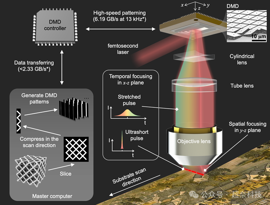
Line-TF TPL technology is based on line illumination by a digital micromirror device (DMD) and spatiotemporal synchronous focusing of femtosecond laser pulses, achieving the following three major technological breakthroughs:
1. True Continuous 3D Nanolithography
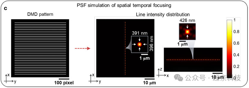
Line-TF TPL achieves true continuous 3D nano printing for the first time. The system focuses femtosecond laser pulses into programmable line patterns and combines continuous linear scanning of the substrate, eliminating the “stop-move-stop” cycles of traditional methods.
The technical core lies in:
- The DMD performs temporal defocusing of the light beam in the x-z plane
- The negative cylindrical lens forms a virtual focal line in the y-z plane
- Spatiotemporal synchronous focusing is achieved through a 4-f system
- Line patterns can be programmed in real time at a 13 kHz refresh rate
This design enables the system to operate continuously at the hardware’s maximum rate, achieving a real-time voxel rate of 3.3 × 10⁷ voxels per second (with 1,600 grayscale levels per voxel), corresponding to a sustainable volumetric printing rate of 0.11-7.6 mm³/hour (when using a 40× objective). When using a 10× objective, the printing rate can reach as high as 950 mm³/hour.
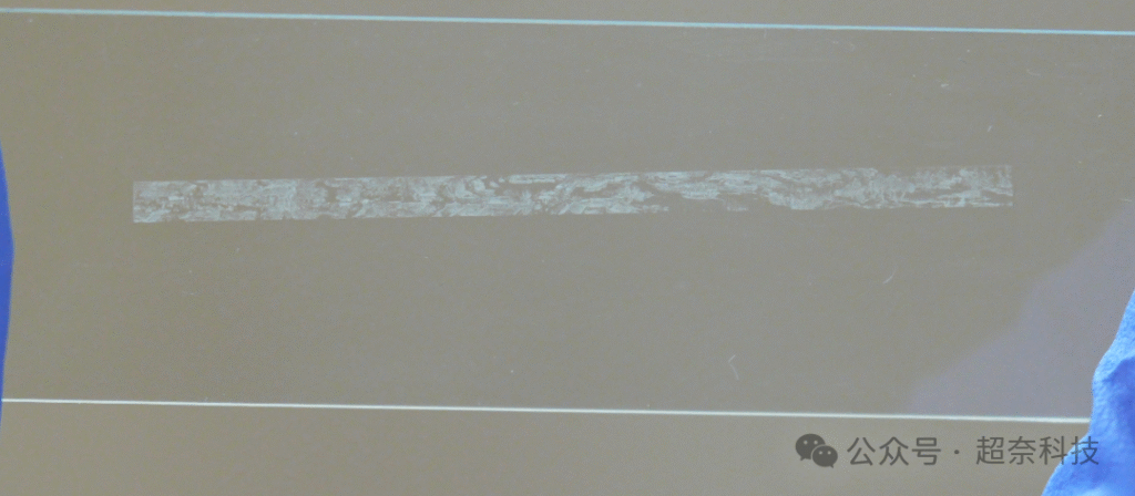
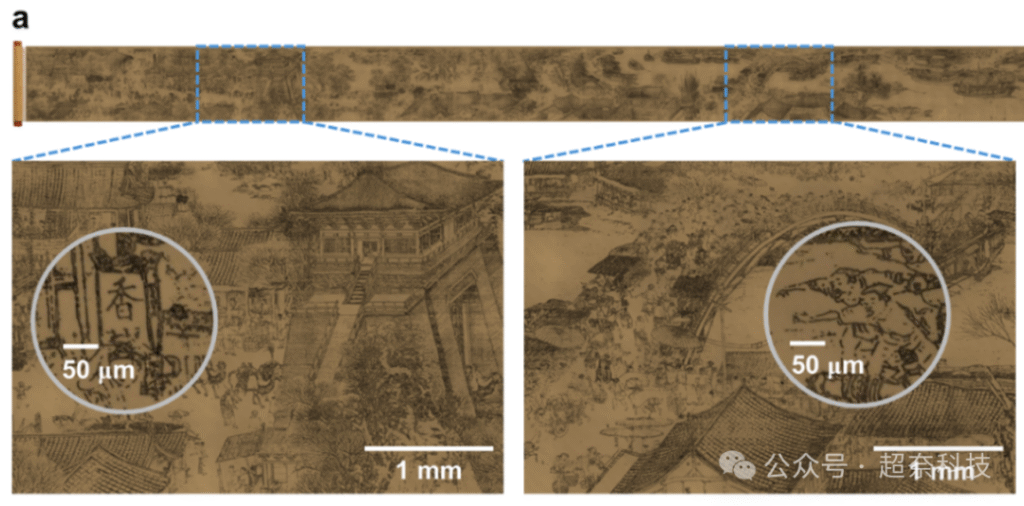
Image: Along the River During the Qingming Festival printed in line-scanning mode
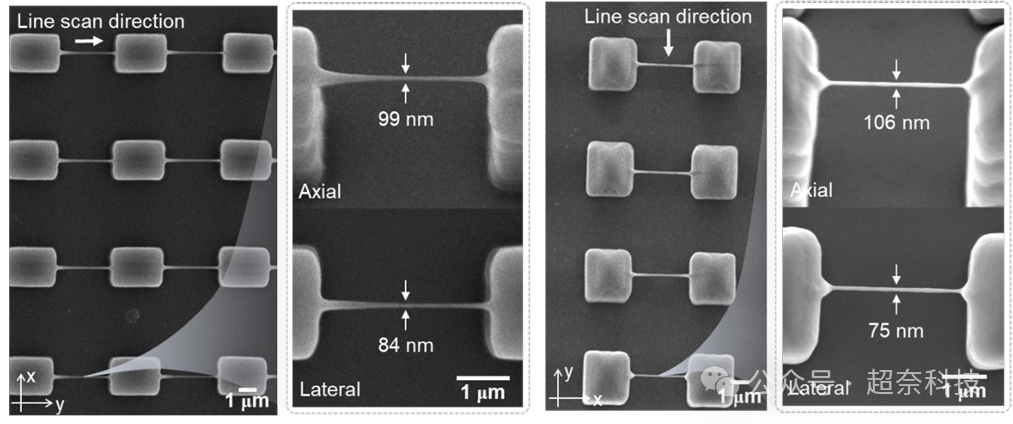
2. Pixel-Level Grayscale Control Capability
Unlike traditional binary modulation of DMD, Line-TF TPL achieves true pixel-level grayscale control. By precisely controlling the number of DMD pixels turned on/off in the y-axis direction, the grayscale intensity of the line pattern can be dynamically adjusted.
This capability brings significant advantages:
- Sub-diffraction feature fabrication: Experiments have confirmed the ability to fabricate suspended nanowires with a lateral width of 75 nm and axial width of 99 nm
- Uniformity compensation: Through grayscale adjustment, the coefficient of variation of line intensity is reduced from 21.93% to 1.26%
- Gradient stitching: Gradually reducing exposure dose at the edges of scanning strips achieves seamless stitching
- Isotropic resolution: Through spatiotemporal focusing, the optical resolution in all three axial directions approaches 400 nm
3. Full-Bandwidth Data Stream Transmission
Line-TF TPL has developed innovative data compression and streaming protocols, effectively solving the data transmission bottleneck:
Data compression strategy:
- After slicing the CAD model, identify unique line patterns within the scanning area
- Transmit only unique DMD patterns, significantly reducing data volume
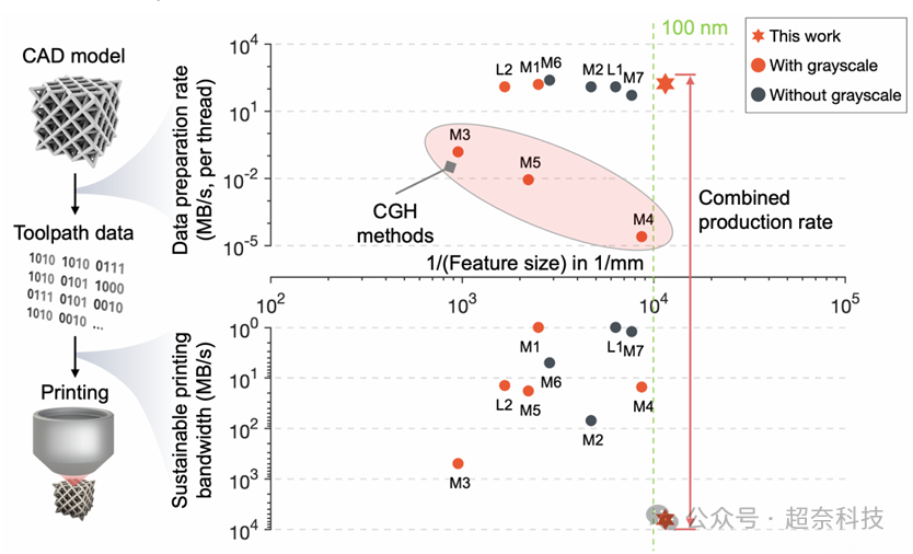
- Through compression factor η, the effective data transfer rate can reach 2.33 × η GB/s (upper limit 6.19 GB/s)
Real-time streaming mechanism:
- DMD memory partition management (projection area, preparation area, upload area)
- Achieve continuous operation by uploading while projecting
- Data preparation rate reaches 168 MB/s per CPU thread (further improvable through multi-core parallelism)
In contrast, for holographic multi-focus TPL systems based on computer-generated holography (CGH), due to the iterative phase retrieval process, the data preparation rate is only 0.15 MB/s per CPU thread, far below the printing rate, resulting in increased equipment idle time.
Technical Advantage Comparison
The sustainable printing bandwidth of Line-TF TPL is 12.7 times higher than existing technologies, while significantly reducing laser cost and adoption barriers.
| Technical Indicator | Line-TF TPL | Projected Light Sheet | Holographic Multi-focus |
|---|---|---|---|
| Lateral/Axial Resolution | 75/99 nm @780 | 142/174 nm | 90 nm @800 |
| Sustainable Printing Bandwidth | 2,393×η MB/s (up to 6,341 MB/s) | 1 MB/s | 15 MB/s |
| Data Preparation Rate | 168 MB/s | 123 MB/s | 2.5 × 10⁻⁵ MB/s |
| Grayscale Capability | Pixel-level control | None | Algorithm-limited |
| Seamless Stitching | X-Y dual axis | None | None |
| Pulse Energy | 50 nJ | 4 mJ | 4 mJ |
| Laser Cost (USD) | ~$120,000 (oscillator) | ~$250,000 (amplifier) | $250,000 |
Application Case Demonstrations
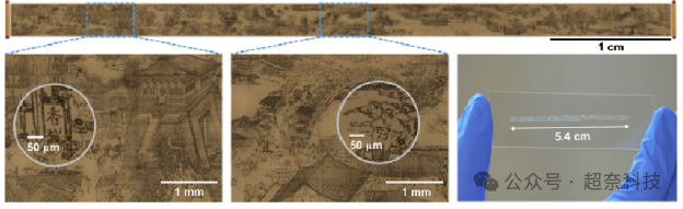
Centimeter-Scale Miniature Artwork – Replica of “Along the River During the Qingming Festival”
- Size: 5.4 cm
- Manufacturing time: 3 hours
- Features: Sub-micrometer resolution, no visible stitching defects, showing fine details such as Chinese characters, figures, trees, etc.
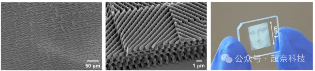
Monochrome Image – “Mona Lisa”
- Size: Centimeter scale
- Manufacturing time: 8 hours
- Technology: Grayscale rendering achieved through dithering distribution of 3D woodpile metamaterials
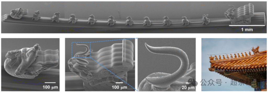
Smooth Surface – Roof Ridge Beast of the Hall of Supreme Harmony in the Forbidden City
- Size: 1 cm
- Manufacturing time: 13 hours
- Features: Each ridge beast has a unique shape with clear details (such as dragon horns), smooth surface
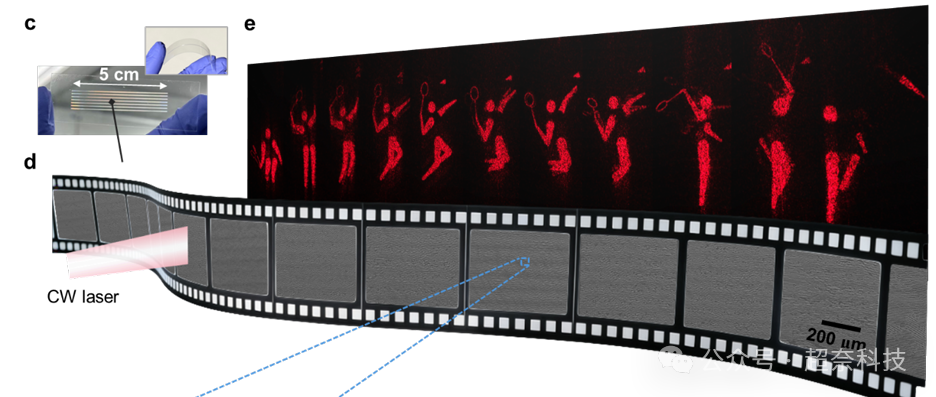
Micro-Optical Device – Continuous Holographic Structure
- Size: 5 cm long film containing 100 holographic frames
- Each frame: 500 × 500 pixels, 1-micrometer pixel size
- Manufacturing time: 13 minutes
- Function: Produces corresponding diffraction patterns under red light illumination, enabling holographic display sequences
- Through gradient overlapping stitching strategy, undesirable artifacts between scanning strips are eliminated, achieving high-fidelity holographic display. This technology can also be printed on flexible PET substrates, and combined with roll-to-roll manufacturing, is suitable for large-scale 3D holographic film production.
Industrialization Prospects
- Photonics packaging: Providing efficient solutions for photonic chip interconnection, particularly suitable for application scenarios such as photonic wire bonding (PWB)
- Metamaterials discovery: Rapidly fabricating complex nanostructure arrays, accelerating the research, development, and optimization of new metamaterials
- Biomedicine: Manufacturing microfluidic chips, tissue engineering scaffolds, drug delivery carriers, and other precision biomedical devices
- Micro-optics and microelectronics: Producing microlens arrays, gratings, waveguides, and other micro-optical components, as well as 3D microelectronic packaging structures
- Information encoding and anti-counterfeiting: Utilizing continuous holographic film technology to achieve large-scale information encoding and 3D holographic anti-counterfeiting labels
We believe that Line-TF TPL technology will not only solve the industrialization challenges of 3D nano printing but also open a new era of large-scale applications in cutting-edge fields such as photonic integration, artificial intelligence, and quantum computing.
Astra Optics Limited will continue to invest in the research, development, and application promotion of advanced nano printing technologies such as Line-TF TPL, working hand in hand with industry and academia to jointly promote the innovation of 3D nano manufacturing technology and contribute to the development of next-generation high-tech industries.
Reference: Zhong, Q., et al. (2024). Full-bandwidth, continuous, and grayscale 3D nanolithography via line-illumination temporal focusing of ultrafast lasers. arXiv preprint arXiv:2512.22746.