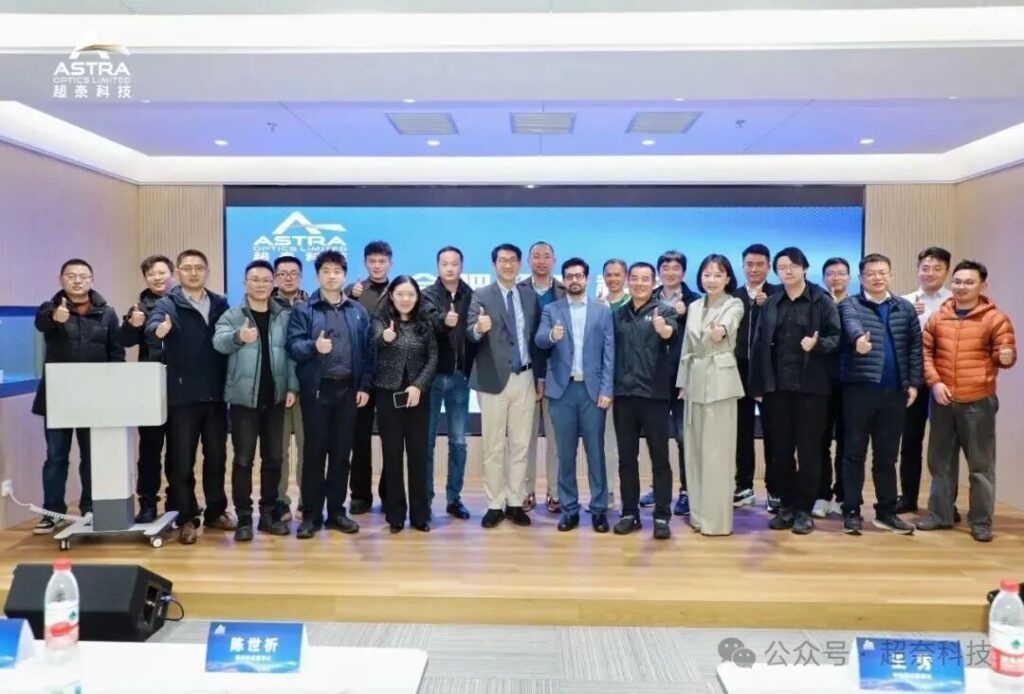
Recently, the new product launch conference of Hefei Astra Optics Limited was successfully held in Hefei. The company’s Chief Technology Officer, Zhong Qiuyuan, officially unveiled two flagship products of Astra Optics Limited at the conference – the LINESCAN 100i Full-Bandwidth Continuous Grayscale 3D Nanolithography System and the UV SCAN 100 UV Laser Direct Write Lithography Machine, marking a key step forward for China in the field of micro-nano manufacturing equipment. Professor Shih-Chi Chen, founder and chairman of the company, attended the conference and delivered a speech. Leaders, experts, and media guests from government departments, research institutions, and the industry gathered together to witness this important moment.
Ten Years of Hard Work: From Science Paper to Mass Production Equipment
In the field of nano 3D printing, traditional two-photon technology has long relied on the “point-scanning” working principle – high precision, but extremely slow and costly. Printing a millimeter-scale device often takes several weeks, with costs reaching tens of thousands of yuan. Bottlenecks such as slow speed, stitching defects, bandwidth limitations, and expensive hardware have severely restricted the industrialization process of this cutting-edge technology.
As early as 2015, Professor Shih-Chi Chen’s team began exploring a path to break the deadlock, laying the foundation for beam shaping with DMD and binary holography technology. After years of tackling key challenges, in 2019 the team successfully developed a femtosecond surface-projection two-photon lithography system, and the relevant results were published in the top international academic journal Science and received the R&D 100 Award in 2018. Subsequently, the team achieved multi-material surface-projection manufacturing in 2022, broke through multi-focus parallel lithography in 2023, and completed the surface-projection two-photon lithography prototype in 2024, achieving a 1,000-fold speed increase, 10-fold resolution improvement, compatibility with more than 20 materials, and one-tenth the cost. In 2025, the team finally conquered full-bandwidth, continuous, grayscale 3D nano lithography technology – a clear and determined ten-year research and development path.
In his speech, Professor Shih-Chi Chen stated: “If research results cannot be translated into practical applications, they will ultimately remain in the laboratory. How to truly transform the ‘from 0 to 1’ technological breakthroughs made in the laboratory into industrial applications and achieve the value leap of ‘from 1 to N’ has always been the core proposition I have been thinking about. Today’s launch is our most resolute answer to this question.”
LINESCAN 100i: Redefining the Future of Nanomanufacturing
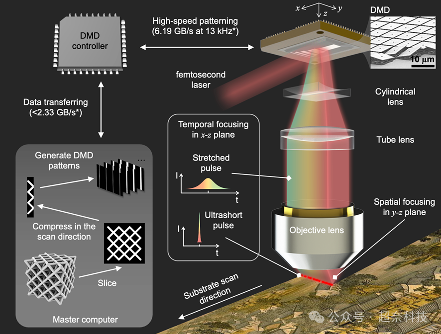
As the core product of this launch conference, the LINESCAN 100i is a full-bandwidth continuous line-illumination spatiotemporal focusing 3D nanolithography system, designed specifically for scientific research exploration and small-batch production, providing a full-bandwidth continuous, grayscale precision control, sub-100-nanometer seamless 3D nanolithography solution.
In terms of core parameters, the LINESCAN 100i achieves three-dimensional uniform ultra-high resolution with a lateral resolution of 75 nm and an axial resolution of 99 nm, an optical bandwidth of 6.19 GB/s, a data transmission rate of 2.33 GB/s, a DMD refresh rate exceeding 10 kHz, and a maximum scanning range reaching the centimeter scale.
Behind these numbers lies the embodiment of five core technical advantages. First, the system adopts continuous scanning and grayscale stitching technology to achieve uninterrupted manufacturing, completely eliminating the stitching defects brought by the traditional “stop-start” mode, resulting in a smoother and more perfect finished product surface. Second, the system supports 1600-level pixel grayscale adjustment. By precisely controlling the switching state and number of each pixel on the DMD, it can manufacture structures with continuously varying material properties, such as smooth-surfaced microlenses and gradient refractive index optical elements. Third, the three-dimensional uniform resolution brought by spatiotemporal focusing technology has highly uniform axial resolution, superior to traditional two-photon lithography. Fourth, the continuous printing bandwidth is 6.19 GB/s, with a data preparation rate of 168 MB/s (per thread), far exceeding similar parallel TPL methods, matching high printing throughput and avoiding machine idle time. Fifth, the line-scanning strategy significantly reduces the requirement for laser pulse energy, eliminating the need for expensive millijoule-level amplifier systems, allowing the use of domestically produced lasers. The continuous manufacturing mode enables equipment utilization close to 100%, significantly reducing usage costs.
At the application level, the LINESCAN 100i has already demonstrated powerful cross-scale, cross-field enabling capabilities. In the manufacturing of precision micro-optical elements, the system can produce high-fidelity grayscale holographic films on glass or flexible substrates, and can also create smooth-surfaced microlens arrays on chips through overlay printing – a core component of AR/VR devices. In the field of fine artwork manufacturing, the system has successfully produced centimeter-scale fine 3D artworks, achieving a perfect leap from the micro-nano scale to macroscopic structures, fully demonstrating the technology’s outstanding ability to manufacture complex structures on a large scale while maintaining ultra-high resolution.
UV SCAN 100: Opening a New Paradigm for Micro-Nano Manufacturing
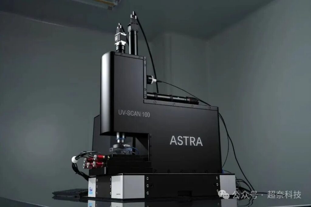
Launched concurrently, the UV SCAN 100 is an ultra-high cost-performance 2-inch UV laser direct write lithography machine, designed specifically for scientific research exploration and small-batch production. It is compatible with gloveboxes, providing flexible and high-precision micro-nano processing solutions.
The UV SCAN 100 adopts maskless laser direct write technology, using a 405 nm UV laser as the light source, achieving a minimum line width of 0.25 μm, approaching the physical diffraction limit. The system’s processing area is 48 mm × 48 mm, with a processing speed of 18 mm²/h, auto-focus accuracy of ±0.2 μm, repeated positioning accuracy of ±0.12 μm. It supports various substrates such as silicon wafers and glass (with vacuum adsorption), and comes equipped with the self-developed AstraWrite software system.
Four differentiated advantages of this product are particularly impressive. In terms of size, the main body of the equipment weighs only 12 kg, with dimensions of only 463 × 160 × 535 mm³. Compared to competitors’ “behemoths” often weighing 597 kg or even 1,000 kg, the UV SCAN 100 can be easily placed inside a glovebox for operation. This means researchers can directly perform micro-nano processing of air-sensitive materials such as perovskites and quantum dots within an inert atmosphere or high-cleanliness glovebox, without needing to transfer samples to external equipment, fundamentally avoiding the risk of material degradation. This capability is extremely rare among similar products, truly achieving “desktop” lithography.
In terms of precision, the system adopts domestically produced high-performance lasers, acousto-optic modulators, galvanometer systems, and a self-developed high-precision optical system, combined with a nano-scale precision motion stage, achieving processing capability close to the physical diffraction limit. In terms of operation, the AstraWrite software supports gradient power and focus offset exposure parameter arrays, allowing one-step screening of optimal exposure parameters, and supports one-click sample loading, auto-focus, auto-alignment, and auto-exposure for the entire process flow. In terms of price, the selling price is only 800,000 to 1.2 million RMB. Compared to the international competitor Heidelberg DWL 66+, which costs around 3 million RMB, it achieves similar or even better performance at less than half the price.
The UV SCAN 100 is suitable for chip rapid prototyping, small-batch trial production, and precision processing in areas such as IC substrates and advanced packaging (RDL/TSV) in the semiconductor and integrated circuit field. It also widely covers the micro-optics and AR/VR field, supporting high-precision processing and manufacturing of gratings, diffractive optical elements (DOEs), as well as in-situ patterning and forming of nanocrystals such as quantum dots and perovskites.
Rooted in Hefei, Innovating for the Future
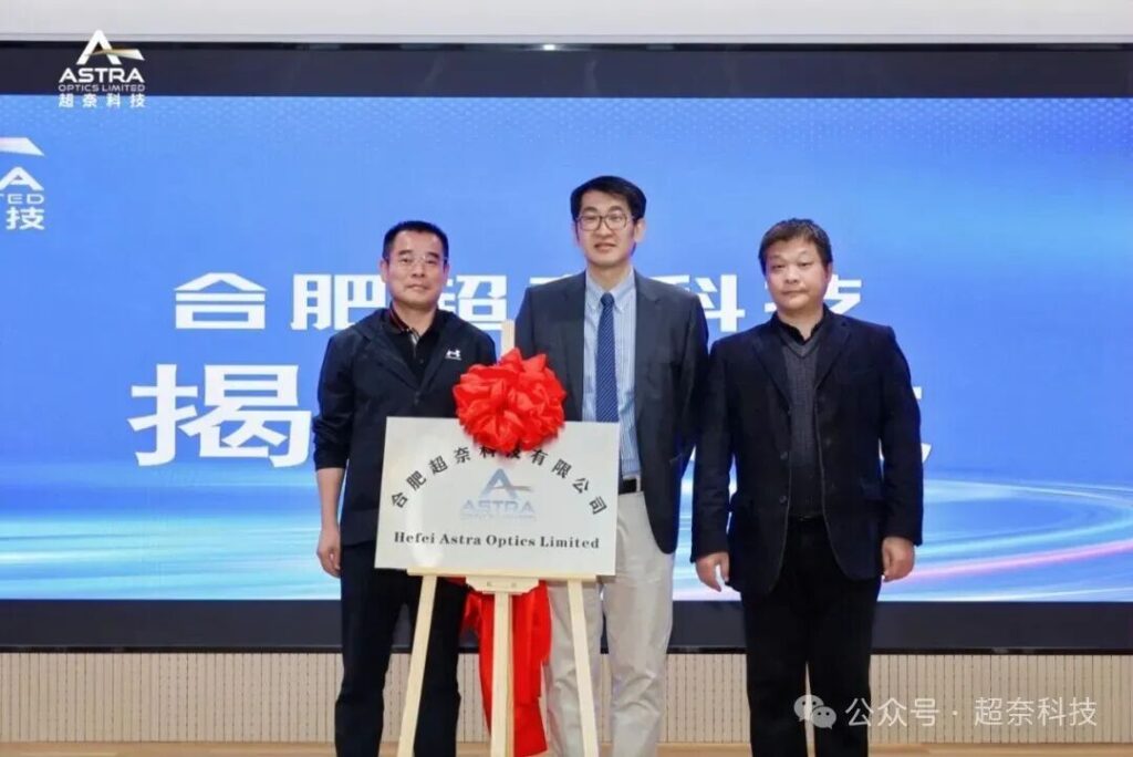
Astra Optics Limited was established in August 2024, landing in Hefei’s KD Innovation Valley (University of Science and Technology of China Silicon Valley). It has received support from theKD Innovation Valley sub-fund and the Hefei Seed Fund. In just one and a half years since the company’s establishment to the simultaneous launch of two heavyweight products, Astra Optics Limited has grown into a hard-tech enterprise with a globally leading product line. Both devices had already won bids for university procurement projects before their official launch, fully validating the technical strength of the products and also marking the initial recognition of domestically produced solutions in the high-end research market.
In his speech, Professor Shih-Chi Chen specifically thanked the Hefei Municipal Government, the High-tech Zone Management Committee, and KD Innovation Valley for their strong support: “We deeply feel Hefei’s industrial warmth of ‘not only attracting investment, but also emphasizing talent cultivation.’ It is precisely the strong support of the Hefei government that has allowed us to grow into a hard-tech enterprise with globally leading products in just one and a half years.”
Looking to the future, Astra Optics Limited will continue to be rooted in Hefei, relying on Hefei’s strong industrial ecosystem and first-class science and innovation environment, continuously promoting product iteration and technological upgrading, allowing Chinese-made micro-nano printing equipment to serve global innovators, and contributing to Hefei’s efforts to build an internationally influential micro-nano manufacturing industrial cluster.