

In the ongoing development of artificial intelligence, the conflict between computing power and energy consumption is becoming increasingly prominent.Imagine a future scenario: drones, autonomous driving systems, or mobile terminals no longer need to rely on high-power AI chips. Instead, with only a transparent nanostructured film placed in front of the camera lens, they could complete visual information processing at the speed of light.Professor Shi-Qi Chen’s team and Professor Chao-Ran Huang’s team at The Chinese University of Hong Kong are gradually bringing this vision closer to reality by deeply integrating manufacturing technologies with optical computing architectures.
I. Industry Challenge: Overburdened Electronic Computing Power
The dependence of traditional machine vision architectures on electronic computing power is structural.
After high-resolution sensors in imaging systems capture images, the information must first be converted into digital signals and then transferred to GPUs for subsequent computation.
Facing the continuously increasing computational demands of deep learning models, the Von Neumann architecture has already demonstrated bottlenecks in areas including:
- Computing speed;
- Power consumption;
- Data storage.
II. The Solution: Optical Neural Networks and Random Projection
To overcome this bottleneck, researchers have turned their attention to Optical Neural Networks (ONN).
Free-space optical processing offers advantages including:
- High speed;
- Low power consumption;
- Natural parallelism.
It is therefore an ideal physical platform for supporting machine vision computing.
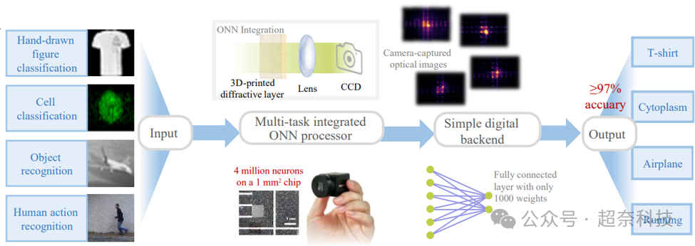
Its operating principle is based on a simple and effective mathematical concept — Random Projection:
Through physical fabrication, a diffractive optical element (DOE) with a random phase distribution is created, whose surface is covered with random nanostructures at the subwavelength scale.
When a coherent optical field carrying image information passes through this 3D-printed diffractive layer, diffraction and interference occur within the nanostructures.
At the moment the light penetrates through the device, a large-scale high-dimensional feature mapping is completed, encoding the original image into a speckle pattern in the Fourier domain.
Mathematically, the Johnson–Lindenstrauss lemma guarantees that random linear projection can preserve the distance relationships between data points while reducing dimensionality, making it an efficient feature encoding method.
More importantly, this computational process is naturally completed through light propagation, consuming no additional electrical energy except for illumination.
The most intensive matrix operations are outsourced to the physical world itself.
III. Manufacturing Breakthrough: Printing 4 Million Optical Neurons in 15 Minutes
Although the concept of Optical Neural Networks (ONN) is promising, their implementation in the visible light spectrum has long been limited by manufacturing technologies.
Visible light has a short wavelength, requiring devices to possess feature sizes at the scale of hundreds of nanometers and extremely high neuron density.
Meanwhile, conventional approaches such as Electron Beam Lithography (EBL) are costly and require several hours…
The work of Wenqi Ouyang and Wen Lyu, co-first authors of the paper, directly addresses this manufacturing challenge by proposing a systematic solution:
Randomized Multi-focus Parallel Printing:
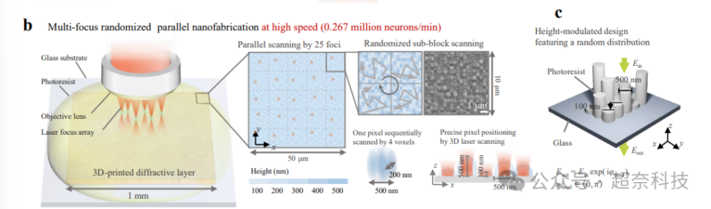
The team independently developed a randomized multi-focus two-photon lithography (TPL) system, which uses Digital Micromirror Device (DMD) holography to reshape femtosecond laser light into 25 parallel focal points, abandoning the traditional single-point sequential scanning approach.
At the same time, the team introduced an original random scanning strategy, which spatially and temporally disperses the exposure of adjacent pixels. This effectively suppresses pixel adhesion and boundary blurring caused by polymerization diffusion, achieving a balance between pixel fidelity and fabrication efficiency.
Fabrication Speed:
The system writes at a speed of 267,000 neurons per minute.
It requires only 15 minutes to fabricate a diffractive layer containing 4 million neurons (500-nanometer units) over an area of 1 square millimeter.
The entire process requires no cleanroom environment.
Combined with PDMS soft lithography and UV nanoimprint lithography, the system can further achieve low-cost mass replication.
Multi-task General-purpose Vision:
As a task-independent universal optical encoder, this optical front-end only requires a single-layer digital readout network containing 1,000 parameters to perform multiple visual tasks, including:
- Handwritten digit classification;
- Object recognition;
- Human action recognition;
- Flow cytometry image classification;
- Facial landmark detection.
All classification tasks achieve an accuracy of ≥97%.
When switching between tasks, only the lightweight digital backend needs to be retrained, while the optical component requires no modification.
IV. Technical Landscape: The Line-scanning Approach from the Same Research Team
In addition to multi-focus parallel printing, Professor Chen’s team has also developed another technical route:
Line-illumination Temporal Focusing Two-photon Lithography (Line-TF TPL),
further expanding the toolbox for high-throughput TPL.
From “Point Arrays” to “Line Scanning”:
This system uses a DMD to simultaneously focus femtosecond laser light in both spatial and temporal dimensions, forming a programmable line-shaped optical field.
Continuous Scanning Printing:
During continuous movement of the sample stage, the line-shaped optical field simultaneously writes patterns, enabling continuous and seamless large-area fabrication.
Grayscale Control and Cost Optimization:
The system supports pixel-level grayscale control, allowing precise regulation of nanostructure morphology.At the same time, it significantly reduces the required pulse energy, making it possible to use lower-cost femtosecond oscillators instead of amplifiers.Multi-focus randomized printing and line-scanning continuous printing are designed for different device requirements and manufacturing scenarios.
V. Scaling Effect: When the Number of Neurons Reaches the Tens of Millions
The maturation of manufacturing technologies for large-scale neuron arrays provides a solid foundation for the scaling of optical computing architectures.
Professor Chao-Ran Huang’s team’s previous research has already demonstrated that when the number of neurons in an optical metasurface reaches the scale of 41 million, a qualitative transformation emerges from quantitative growth:
A completely untrained static random metasurface can achieve feature encoding capabilities comparable to large electronic AI models such as ResNet and Vision Transformer.
This discovery establishes, from a fundamental perspective, the feasibility and competitiveness of the architecture:
“Large-scale random optical encoding + lightweight digital readout.”
Following this direction, the future application landscape has become increasingly clear:
By leveraging high-speed, low-cost 3D nanoprinting and imprint replication technologies, the “photonic neural metasurface” is expected to achieve large-scale production similar to optical coatings.
It could be directly integrated into:
- Smartphones;
- Miniature medical endoscopes;
- Autonomous driving cameras.
At the same moment the device captures light, it can complete feature extraction and visual computing with extremely low power consumption.
From electronic computing toward optoelectronic integration, this 3D-printed diffractive film may become an important foundation for crossing into a new computational paradigm.
Reference:
Multi-task large-scale integrated optical vision processor using ultra-fast parallel nanofabrication
Light: Advanced Manufacturing