In today’s rapidly developing photonic chip industry, how to achieve efficient interconnection between chips and between chips and optical fibers has always been a major challenge faced by the industry. Traditional packaging processes are not only costly but also require extremely high alignment precision, becoming a bottleneck restricting the large-scale application of photonic integrated circuits. An innovative technology based on 3D nano printing – Photonic Wire Bonding (PWB) – is bringing a breakthrough solution to this problem.
Image source: Vanguard Automation
The Dilemma of Photonic Chip Packaging
The photonic integrated circuit (PIC) market is expanding rapidly with a compound annual growth rate of 25.9%, showing enormous potential in fields such as data communications, 3D sensing, and quantum applications. Even so, the packaging and assembly of photonic chips still face challenges.
The mode field size differences between different optical platforms are enormous. The core diameter of a single-mode fiber is approximately 10 micrometers, while that of a silicon-based photonic waveguide is only about 1 micrometer. This significant size difference requires extremely high alignment precision, and traditional packaging methods often require complex micro-optical elements and precise assembly processes.
More critically, packaging costs account for more than 70% of the total cost of photonic integrated systems. This high cost severely restricts the large-scale commercial application of photonic chip technology.
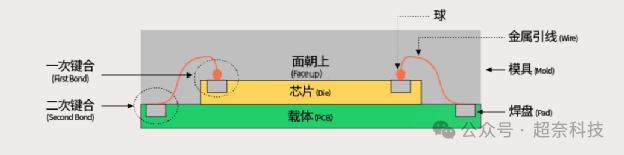
Image source: SK Hynix
PWB Technology: An Innovative Application of 3D Nano Printing
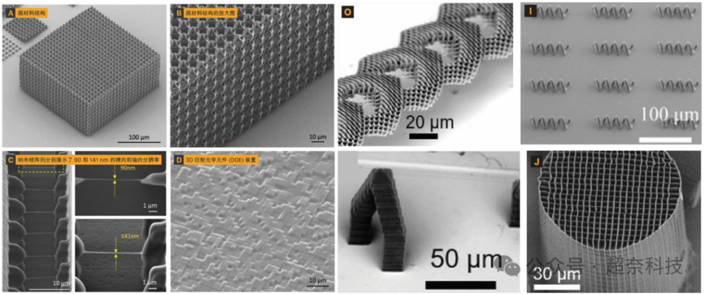
Photonic Wire Bonding (PWB) technology is based on the two-photon polymerization (TPP) 3D nano printing process, providing a revolutionary solution for photonic chip interconnection.
The working principle of this technology is: using femtosecond laser to perform high-precision three-dimensional printing in photosensitive resin, directly “building” polymer optical waveguides between chips and optical fibers. These micrometer-scale optical waveguides, like gold wire bonding in electronic chips, achieve efficient transmission of optical signals.
Image source: Protoexpress
Technological Breakthroughs: From Theory to Practice
A study recently published in the journal Materials demonstrates the latest progress in PWB technology. The research team developed an innovative in-situ multi-physics measurement method capable of simultaneously monitoring the mechanical properties and optical transmission characteristics of PWB in a scanning electron microscope (SEM).
This research revealed the key elements of PWB structural design:
- Geometric optimization: By precisely controlling the size and length of the tapered structure and the radius of curvature of the bonding part, optical loss can be significantly reduced. The study shows that when the taper width is 14 micrometers, the length is 75 micrometers, and the bonding radius of curvature is greater than 30 micrometers, optimal optical transmission performance can be achieved.
- Mechanical toughness: PWB not only needs low optical loss but must also possess sufficient mechanical strength to withstand subsequent process steps. Experiments found that photonic wires with smaller radii of curvature have better elastic recovery capability, being able to fully recover their original shape even after vertical compression of 20 micrometers.
- Optical recoverability: Even more excitingly, the study confirms that the optical loss of PWB within the elastic deformation range is completely reversible. When the external force is removed, the optical waveguide not only recovers its original shape but also completely recovers its optical transmission performance, providing an important guarantee for the reliability of PWB in practical applications.
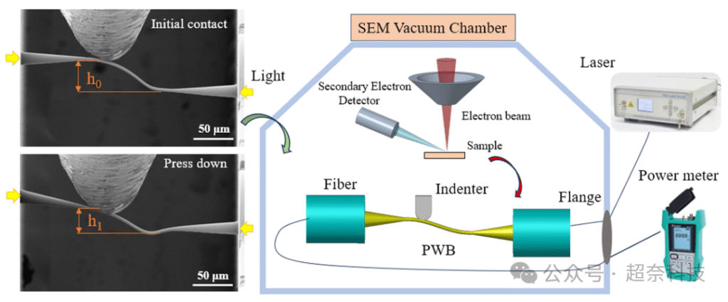
Image source: Materials
Industrial Application Prospects
PWB technology has already demonstrated practical application value in multiple fields:
- In the field of optical communications, PWB provides an ideal solution for high-density optical interconnection, capable of achieving multi-channel parallel transmission in compact spaces.
- In quantum photonics, the low-loss characteristics of PWB are crucial for single-photon-level signal transmission, laying the foundation for the development of quantum computing and quantum communication.
- In optoelectronic integration, PWB technology can achieve efficient interconnection between different functional devices such as lasers, modulators, and detectors, promoting the development of heterogeneous integration technology.
Astra Optics Limited: Driving the Industrialization of PWB Technology
As a pioneer in 3D nano printing technology, Astra Optics Limited is committed to promoting the industrial application of advanced technologies such as PWB. We have industry-leading 3D nano printing equipment and complete process solutions, providing full-process services from design optimization to mass production for photonic chip packaging.
Our technical advantages include:
- Ultra-high precision printing: Using advanced surface projection technology to achieve nanoscale resolution in 3D structure manufacturing
- Comprehensive process support: Providing full-range technical services from material selection, structural design to performance testing
- Industrial-grade reliability: Ensuring products meet strict industrial application standards
Looking Ahead
As photonic chip technology continues to develop, the requirements for packaging and interconnection technology are also constantly increasing. With its unique advantages, PWB technology is expected to become the mainstream solution for next-generation photonic integrated circuit packaging.
In the future, with further improvements in printing precision, the development of new optical materials, and the refinement of automated production processes, PWB technology will achieve greater breakthroughs in the following directions:
- Achieving lower optical loss (<0.5 dB)
- Supporting larger-scale parallel interconnection
- Extending to wider wavelength ranges
- Reducing production costs and increasing yield
Astra Optics Limited will continue to invest in the research, development, and application promotion of 3D nano printing technologies such as PWB, working hand in hand with industry and academia to jointly promote the innovation of photonic chip packaging technology, contributing to the development of cutting-edge fields such as optical communications, artificial intelligence, and quantum computing.
We believe that 3D nano printing technology will not only solve the problem of photonic chip interconnection but also open a new era of large-scale application of photonic integration technology.
References:
Lei, Y., et al. (2024). In Situ Multiphysical Metrology for Photonic Wire Bonding by Two-Photon Polymerization. Materials, 17, 5297.
Vanguard Automation. Next Generation Photonic Integration and Packaging Solutions with Photonic Wire Bonding.