As the core of modern electronic industry, chip manufacturing has always had its cost and complexity as important factors restricting the development of the industry. However, a revolutionary technology is bringing a brand new solution to this dilemma – 3D printing technology. This technology is expected to become the next major breakthrough point in chip manufacturing.
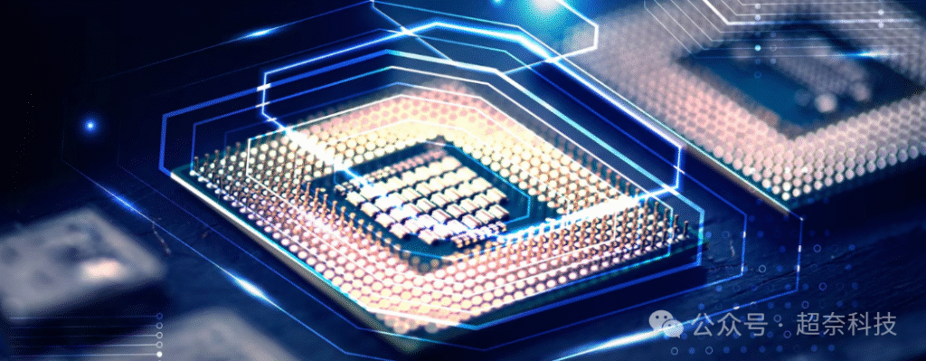
3D Nano Printing Enters the Field of Chip Manufacturing
Recently, an announcement by startup company Atum Works has attracted industry attention. The company stated that its nanoscale 3D printing technology is expected to replace some existing production processes, thereby reducing chip manufacturing costs by 90%.
The nanoscale 3D printer developed by Atum Works can print multi-material 3D structures at 100-nanometer resolution on wafer-level materials. Unlike traditional planar lithography processes, this technology precisely deposits materials into designated positions in three-dimensional space, making the manufacturing of integrated circuits possible and allowing structures such as interconnects to be formed in a continuous process.
However, this technology also has its limitations: although it may be sufficient for applications in packaging, photonics, and sensors, for logic chips, its technology still lags behind current mainstream processes by about 20 years. Current EUV lithography technology has a resolution of approximately 13 nanometers, while technology with 100-nanometer resolution is equivalent to the 90-110 nanometer process level from 2003 to 2005.
Nevertheless, this technological development still demonstrates the enormous potential of 3D nano printing in the field of chip manufacturing.

Image source: Atum Works
Difficulties and Challenges of Traditional Chip Manufacturing
To understand the significance of 3D nano printing technology, we first need to recognize the challenges faced by traditional chip manufacturing. Jensen Huang, founder of NVIDIA, pointed out that advanced chip manufacturing requires more than 1,000 steps, each of which must be nearly perfect to produce functional output.
Modern chips are similar to buildings, having multiple layers, different types of modules, and complex communication networks. The manufacturing process of every advanced chip is extremely complex, involving thousands of steps and hundreds of specialized tools, thus the manufacturing cost is quite high. Taking NVIDIA’s H100 GPU as an example, the average selling price per chip is as high as $30,000. The high manufacturing cost is also the next major mountain that the semiconductor industry needs to overcome.

Image source: NVIDIA
Technical Advantages of 3D Nano Printing
Compared to traditional manufacturing processes, 3D nano printing technology has multiple potential advantages in the field of chip manufacturing:
- Cost advantage: 3D printing does not require mold opening, eliminating expensive upfront costs, and can flexibly process and print according to the structure of each chip. At the same time, 3D printing technology can reduce the number of steps in the chip processing process, including photolithography, etching, polishing, deposition, etc., thereby saving the cost of a large amount of equipment. The integrated process solves the compatibility issues among various equipment.
- Manufacturing flexibility: Through precise material deposition in three-dimensional space, complex three-dimensional structural designs can be achieved, providing new possibilities for chip architecture innovation.
- Specific application advantages: Although there is still a technological gap in the field of high-performance logic chips, 3D nano printing technology shows good application prospects in fields such as packaging, photonics, interconnect structures, sensors, and non-logic components.
Technological Breakthroughs: From Theory to Practice
Solutions to the precision problem
The precision of traditional 3D printing is generally only 1/10 of a millimeter, while chip manufacturing requires nanoscale precision. In 2022, a research team from Carnegie Mellon University, including Professor Shih-Chi Chen, one of the founders of our company Astra Optics Limited, published a breakthrough research result in the journal Science.
They developed a strategy to create ultra-high-resolution, complex 3D nanostructures using various materials, reducing the size of printable nanodevices to ten-something nanometers. This technology creates three-dimensional patterns of materials in a hydrogel and then shrinks them to achieve nanoscale resolution, reducing the resolution of 3D printing technology by several orders of magnitude.
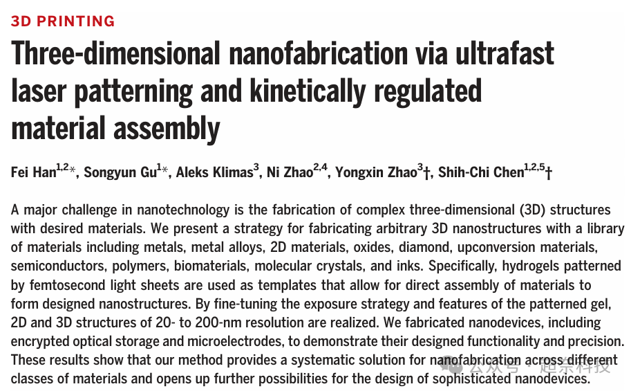
Image source: Science
Industrial Application: Breakthroughs in the Field of Photonic Chips
In the field of photonic chip research, 3D nano printing technology has already demonstrated practical application value. Researchers including Dong Yibo from the Photonic Chip Research Institute used laser nano printing technology to successfully develop a miniature active vortex laser, laying the foundation for the development of orbital angular momentum on-chip information multiplexing technology.
This vertical-cavity surface-emitting vortex laser, which integrates orbital angular momentum phase structures based on laser nano 3D printing, has the advantages of small size, high speed, and low threshold. The size of a single device is only approximately 100 micrometers × 100 micrometers, and the printing time takes only about 20 minutes, which is a significant improvement in efficiency compared to traditional methods. The printers of Astra Optics Limited, using surface projection technology, can further compress the printing time to within 1 minute.
This research solved the problem of increasing the topological charge of miniature vortex lasers and is expected to promote the miniaturization and integration development of orbital angular momentum information multiplexing technology.
Astra Optics Limited: Driving the Development of 3D Nano Printing Technology
As a practitioner of 3D nano printing technology, Astra Optics Limited is committed to promoting the industrial application of this technology. The company has a team composed of industry experts, including renowned scholars such as Professor Chen, who has made important contributions to nanoscale 3D printing technology.
We focus on the research and development of 3D nano printing equipment and the provision of related printing services, providing high-precision 3D nano printing solutions for research institutions and industries, and assisting in the research and application development of related technologies.
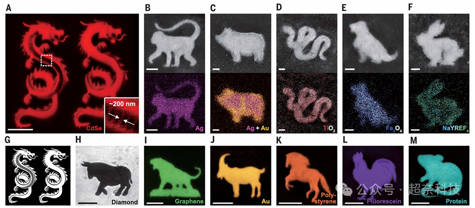
Image source: Science
Looking Ahead: Opportunities and Challenges for Technological Development
Although 3D nano printing technology still faces technical challenges in logic chip manufacturing at present, with continuous improvement in printing precision and the development of new materials, 3D nano printing is expected to bring breakthroughs to logic chip manufacturing.
First, in the prototype verification stage, 3D nano printing can rapidly manufacture chip prototypes, significantly shortening the design verification cycle and reducing early development costs. Second, in specific logic circuit designs, such as three-dimensional stacked structures and complex interconnect networks, 3D printing technology may provide degrees of design freedom that are difficult to achieve with traditional processes.
In the future, with the application of new materials in 3D printing and the development of printing precision toward higher accuracy, we have reason to believe that 3D nano printing technology will eventually play an important role in the field of logic chip manufacturing, and may even give rise to brand new chip architectures and computing paradigms.
Astra Optics Limited will continue to commit itself to the innovation and application of 3D nano printing technology, contributing to the technological advancement of related industries. We believe that with the continuous maturation of the technology, 3D nano printing will bring new possibilities and development opportunities to chip manufacturing.