
In December 2025, the latest research published in the journal Nature by Dr. Songyun Gu of Lawrence Livermore National Laboratory (LLNL) in the United States proposed a parallel 3D nano printing platform based on metalens arrays. This system utilizes microlens units with 100-micrometer apertures to construct an array containing more than 120,000 focal spots, achieving a peak manufacturing rate of 120 million voxels per second over an area of 12 square centimeters, pushing the throughput of large-area nanofabrication to new heights.

The Dilemma of Traditional Parallel TPL Technology
Two-photon polymerization is one of the most advanced 3D nano printing technologies today. Its physical mechanism is based on nonlinear optical effects: when a femtosecond laser pulse is focused inside the photoresist, only the focal spot has sufficiently high light intensity to trigger two-photon absorption, causing the material to polymerize and solidify. This “threshold effect” gives TPL its unique three-dimensional processing capability and sub-diffraction resolution.
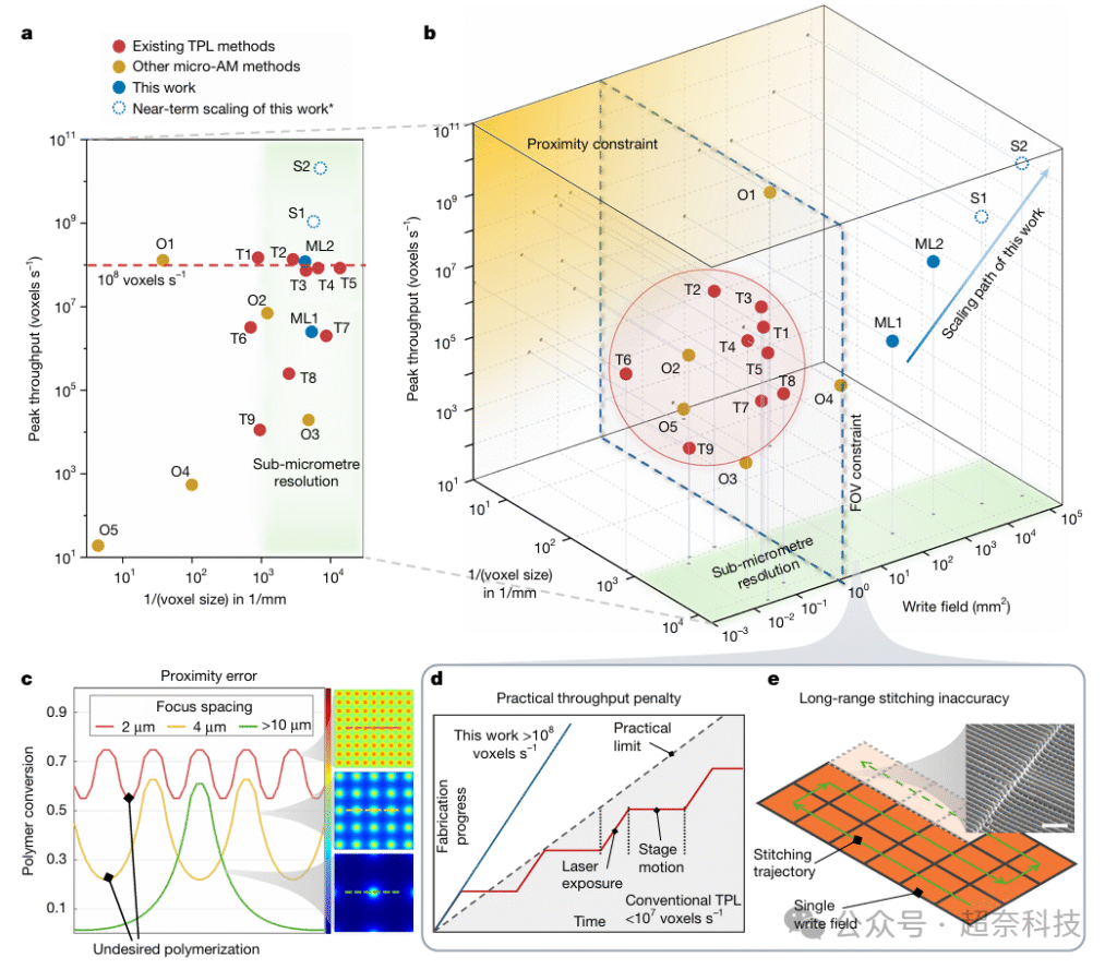
To improve manufacturing rates, researchers have developed various parallel TPL methods, but each has its limitations. Multi-focus holographic printing can achieve simultaneous printing of hundreds to thousands of focal spots, but computing the hologram requires iterative algorithms, resulting in low data processing rates, and the number of focal spots is limited by the resolution of the spatial light modulator. Projected light sheet exposure has fast single-layer exposure speed, but requires high-power laser amplifiers, and the optical field of view is typically less than 1 square millimeter. Microlens arrays have high optical efficiency and simple structure, but dispersion compensation is difficult, and flexibility is poor.
All parallel TPL technologies based on fixed field of view face the same problem: traditional methods adopt an intermittent working mode of “stop-expose-move-stop”. The mechanical vibrations introduced by frequent starting and stopping cause positioning errors, obvious stitching lines appear at the boundaries of adjacent fields of view, and the time spent on moving and stabilizing accounts for 20% to 40% of the total time, resulting in efficiency loss.
Core Innovations
Dr. Songyun Gu and his team’s core innovation lies in abandoning traditional microscope objectives and designing a set of optical systems based on metasurfaces.
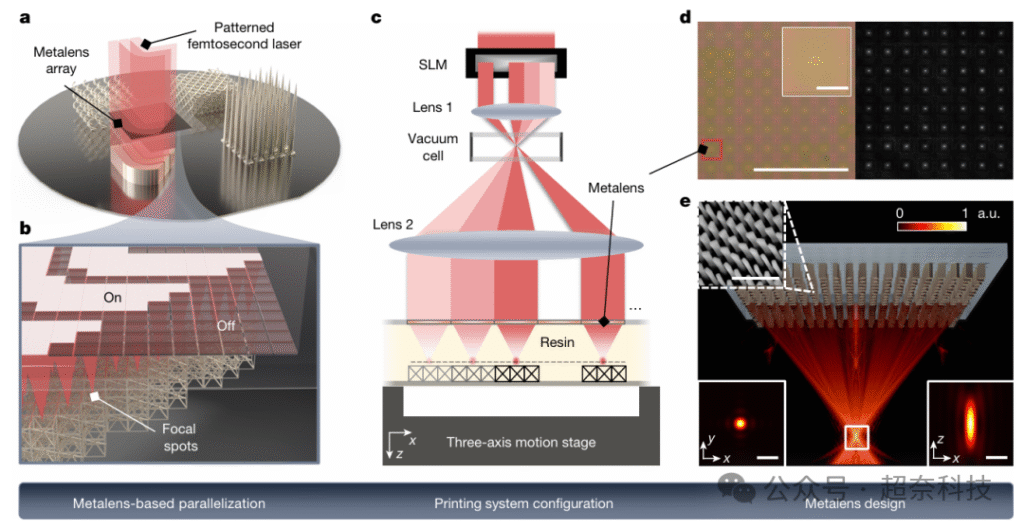
1. Dual-array strategy: The research team designed two specifications of metalens arrays to suit different needs:
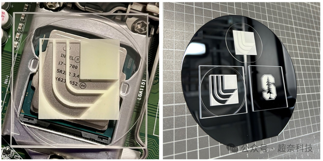
- High-throughput type: Composed of 370 × 350 lenses, with a single lens aperture of 100 micrometers (NA 0.8), total number of focal spots exceeding 120,000, covering 12 square centimeters, specifically designed for large-area rapid manufacturing.
- High-resolution type: Composed of 50 × 50 lenses, with a single lens aperture of 200 micrometers (NA 1.0), used to achieve ultimate printing precision.
2. Metalens design details: Unlike traditional lenses, these metalenses are designed based on the geometric phase principle. They are arrays of polycrystalline silicon nanopillars fabricated on fused silica substrates. Each nanopillar has a height of 785 nanometers, adopts a rectangular cross-section (length 195 nm, width 104 nm), and precisely controls the phase by changing the rotation angle of the rectangle. This design not only achieves high numerical aperture (NA 0.8-1.0) but also utilizes the high refractive index contrast of silicon material to ensure durability in an immersion photoresist environment.
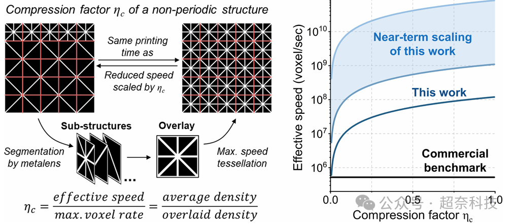
3. Dynamic enabling by spatial light modulator (SLM): Having just the array is not enough. The system introduces a spatial light modulator (SLM) at the front end of the optical path, acting as an “optical switch” and “grayscale controller”. It can independently control the brightness and intensity of these 120,000 focal spots, and combined with a unique adaptive microlithography (AML) algorithm, achieves parallel printing of aperiodic complex structures.
Technical Performance Measurements and Core Indicators
1. Resolution test: Sub-diffraction-limit precise control
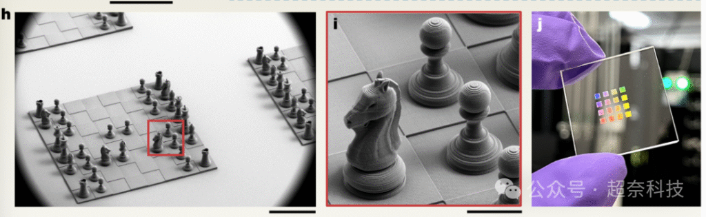
The research team used the SLM to perform fine grayscale control of laser intensity, testing the resolution limit in the sub-threshold region. Experimental results showed that the minimum lateral line width of the printed suspended nanowires was 113 nanometers (axial direction 262 nanometers), and the standard deviation of line width among different metalenses was only 16.5 nanometers (10 repeated experiments). This result not only reaches the precision level of traditional single-focus TPL (typically 100–150 nanometers) but also proves that the system maintains extremely high manufacturing consistency while achieving large-scale parallelization.
2. Large-area stitching: Micron-level stepping eliminates macroscopic errors
In the stitching quality test, the team did not adopt traditional large-range mechanical scanning. Instead, they utilized a strategy where each metalens is responsible only for its sub-region of 100 micrometers or 200 micrometers. By moving the high-precision piezoelectric stage within a small travel range, the system effectively eliminated long-range cumulative errors, controlling the stitching error between sub-fields of view to within 100 nanometers, achieving seamless transitions invisible to the naked eye. Additionally, to address the problem of uneven light intensity across the array, the team developed a grayscale compensation algorithm based on “pixel-level calibration,” ensuring printing consistency across all 120,000 focal spots.
3. Manufacturing rate: A leap in throughput of hundreds of millions of voxels
In terms of manufacturing rate, the peak throughput of this system reaches 120 million voxels per second, covering an area of up to 12 square centimeters (approximately 2-inch wafer size). In contrast, traditional single-focus TPL is limited by field of view and mechanical scanning speed, so actual throughput is often constrained; while existing multi-focus holographic TPL technologies typically face bottlenecks in slow computer-generated hologram generation and proximity effects. LLNL’s metalens array solution achieves effective throughput several orders of magnitude higher than traditional lithography technologies while maintaining sub-micrometer resolution through fully parallel direct writing.
In-depth Analysis of Core Advantages
1. Breakthrough parallelism and scalability
The most intuitive advantage of metalens array technology is its astonishing parallel processing capability. The system integrates approximately 120,000 independently controlled miniature metalenses (100-micrometer units), which is orders of magnitude higher than existing multi-focus scanning systems. This parallel design is not simply a stack of numbers; by eliminating the traditional bulky objective lens, the parallelism becomes linearly scalable – in theory, as long as the wafer area is increased, the number of focal spots can be expanded to the millions without sacrificing resolution.
2. Decoupling the “resolution vs. field of view” contradiction (12 cm² writing area)
Traditional TPL technology, limited by the field of view (FOV) of microscope objectives, typically can only perform high-precision printing within a range of a few hundred micrometers. To fabricate large-sized objects, thousands of mechanical stitching operations are required, which easily introduces errors. This technology adopts a “break the whole into parts” strategy, utilizing 120,000 microlenses to operate simultaneously over a macroscopic area of 12 square centimeters. Each lens is responsible only for its sub-micrometer region below, achieving seamless stitching through short-range high-precision piezoelectric movement. This architecture completely breaks the traditional optical limitation of “high NA inevitably means low FOV,” making wafer-level micro-nano manufacturing possible.
3. Minimalist and independent optical architecture
Unlike holographic multi-focus systems (Holographic Multi-focus TPL) that rely on complex optical paths, the metalens array adopts a non-imaging optical architecture. It does not require Fourier lenses or complex phase modulation optical paths, but directly utilizes metasurfaces for wavefront shaping. More critically, there is the independence of the focal spots: in holographic systems, generating multiple focal spots is often accompanied by complex interference calculations and uneven light intensity, and focal spots that are too close can lead to proximity effects, causing over-polymerization. In the metalens array, the optical field of each lens is physically isolated and non-interfering, and with grayscale control by the SLM, it ensures that the energy distribution of each focal spot is highly uniform and independently adjustable.
Horizontal Comparison with Competing Technologies
1. Comparison with traditional single-focus TPL: trade-off between speed and precision
- Resolution advantage: Traditional single-focus technology is still the king of precision, with a maximum resolution of 50 nm, better than the metalens array’s 113 nm.
- Speed disadvantage: However, there is an order-of-magnitude difference in throughput. The volumetric rate of a single-focus system is only 0.001 – 0.01 mm³/h, while the metalens array system reaches 0.05 – 5 mm³/h.
- Positioning difference: The speed of the metalens array is 500 to 5,000 times that of single-focus. This determines that single-focus technology will continue to dominate the preparation of small-size, ultra-high-precision research samples, while the metalens array fills the manufacturing gap for medium-precision, medium-size functional devices.
2. Comparison with holographic multi-focus TPL: competition between photon efficiency and computing power
- Number of focal spots: Although holographic methods are flexible, the number of independent focal spots, limited by the resolution of the spatial light modulator (SLM), typically does not exceed 10,000, which is only 1/12 of the metalens array (120,000).
- Computational bottleneck: Generating high-quality holograms relies on complex iterative algorithms, making real-time printing difficult, while the metalens array avoids this computational bottleneck through physical masking.
- Optical efficiency: The overall optical efficiency of holographic systems is typically between 20% and 40%, lower than the metalens array’s 49.3%, meaning the latter is more economical in energy utilization.
3. Comparison with projected light sheet TPL: mismatch between cost and application scenarios
- Speed advantage: Projected light sheet technology represents the ultra-high-speed route. It achieves surface-projection printing through spatiotemporal focusing technology, with a volumetric rate of up to 10 mm³/h, outperforming the current metalens array in peak throughput.
- Cost and price: But this speed comes at the cost of expensive hardware. The system relies on a high-power femtosecond laser regenerative amplifier, with the core light source costing as much as 200,000to200,000to500,000.
- Field of view and limitations: Although its resolution can also reach the sub-micrometer level (approximately 140–175 nm), on par with the metalens array, its single-exposure field of view is extremely small (typically far less than 1 mm²).
- Application mismatch: This “small field of view, requiring stitching” characteristic makes it difficult to meet the stringent requirements of large-area photonic chips for seamless connections, making it more suitable for biomedical scaffolds and microfluidics where stitching defects are not sensitive; while the metalens array, with its large-area seamless lithography capability, becomes a better solution for photonics and metamaterial manufacturing.
Technology Heritage and Evolution
Dr. Songyun Gu, the first author of the paper, is now a postdoctoral researcher at LLNL. This research continues his deep accumulation in high-throughput TPL technology. In 2022, while pursuing his PhD in the research group of Professor Shih-Chi Chen at The Chinese University of Hong Kong, Gu published a rapid 3D nano manufacturing method combining femtosecond laser patterning with dynamically controlled material assembly in Science. This newly published research on metalens arrays represents another major breakthrough for Dr. Gu on the parallel TPL technology path. From computational holography to metalens arrays, the research team has always been committed to exploring different technical paths to solve the core challenges of high-throughput nano manufacturing.

Group photo of Dr. Songyun Gu (center) with the team at The Chinese University of Hong Kong
Conclusion
The metalens array parallel 3D nano printing technology of Dr. Songyun Gu and his team is an important milestone in this field. From a scientific contribution perspective, it is a breakthrough: the first realization of 120,000-focus parallel TPL, proving the feasibility of metalenses in high-precision manufacturing. From an engineering maturity perspective, key challenges such as dispersion compensation and system integration still require further optimization, but the technical path is already clear. The industrialization prospects are worth looking forward to: it has unique advantages in specific niche markets such as photonic packaging, metamaterials, and microfluidics, and is expected to achieve large-scale application within 5 to 10 years.
References:
Gu, S., Mao, C., Guell Izard, A., Sadana, S., Terrel-Perez, D., Mettry-Yassa, M., Choi, W., Zhou, W., Yan, H., Zhou, Z., Massey, T., Abelson, A., Zhou, Y., Huang, S., Daraio, C., Tumkur, T. U., Fan, J. A., & Xia, X. (2025). 3D nanolithography with metalens arrays and spatially adaptive illumination. Nature, 648, 591–599.