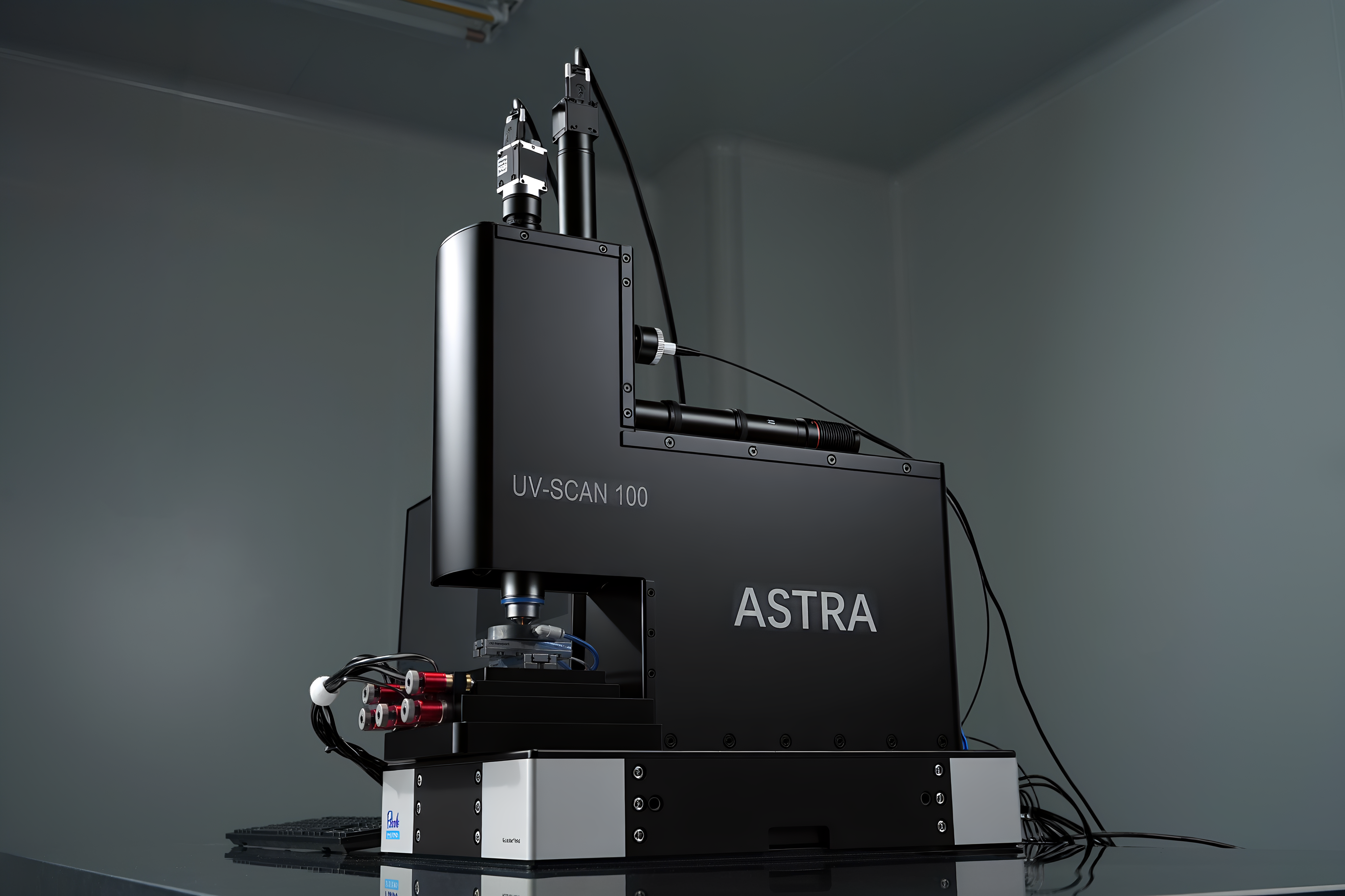
Glovebox-Compatible Laser Direct Writing System
Using dedicated software for micro-nano structure design, the system automatically converts pattern data into control commands to streamline the printing process.
The UV laser beam, modulated by a synergistic AOM and high-precision galvanometer system, is precisely focused onto the photoresist surface through a high-NA objective lens to ensure superior exposure quality.
The laser beam executes high-speed, high-precision point-by-point scanning exposure along the predefined path, delivering stable sub-micron resolution control.
With its compact design, the system can be readily integrated into a glovebox, ensuring stable performance under controlled ambient conditions to support the development and testing of sensitive materials like perovskites.
High-End Hardware, Highly Localized: The system integrates domestically produced high-performance optical components, a proprietary precision optical system, and a nanometer-precision motion stage — together establishing an unparalleled foundation for precision and reliability.
Ultimate precision: minimum linewidth down to 0.25 μm, approaching the physical diffraction limit.
Maskless digital workflow: No expensive physical masks required; design changes are made by simply updating digital files.
Rapid prototyping :Flexibly adapts to complex circuits and fine micro/nano structures alike, enabling fast conversion from concept to prototype, significantly reducing R&D cycle time and costs.
Efficient parameter screening :Supports gradient power and focus offset exposure parameter arrays, enabling rapid identification of optimal process parameters in a single exposure.
One-click automation : Integrates one-click loading, auto-focus, auto-alignment, and auto-exposure, significantly boosting printing efficiency and reducing maintenance costs.
User-friendly interface:Clear and intuitive operation logic minimizes the learning curve.
The UV SCAN 100 delivers exceptional resolution and manufacturing efficiency. Its key performance parameters and application areas are outlined below.
| Application | Two-Photon Polymerization (TPP) Printing Technology |
|---|---|
| Minimum Feature Size (XY) | 250 nm |
| Minimum Equally Spaced Line Grid | 560 nm |
| Writing Rate | 18 mm²/h |
| Exposure Area | ≥ 0.25 mm x 0.25 mm (single processing range, supports stitching for larger patterns) |
| Stitching Error Between Adjacent Exposure | ≤ 150 nm |
| XY Stage Bidirectional Repeatability | ≤ 120 nm |
| Minimum Step Size | ≤ 50 nm |
| Printing Range (XY) | 48 mm x 48 mm |
| Substrate Type | Microscope slides / wafers |
| Substrate Thickness | 0 - 4.5 mm |
| Sample Size | 5 mm x 5 mm to 48 mm x 48 mm (customizable) |
| Vibration Isolation (Optional) | Platform Dimensions ≥ 400 mm × 30 mm; Bandwidth 1–200 Hz; Efficiency > 90% @ 5 Hz, 90% – 99% @ 10 Hz |
| Light Source | 405 nm |
| Length x Width x Height(lithography unit only) | 463 mm x 160 mm x 535 mm |
| Weight (lithography unit only) | 12 kg(backpack-grade) |
| Power Supply | 230 VAC ± 5 %, 50/60 Hz, 16 A |
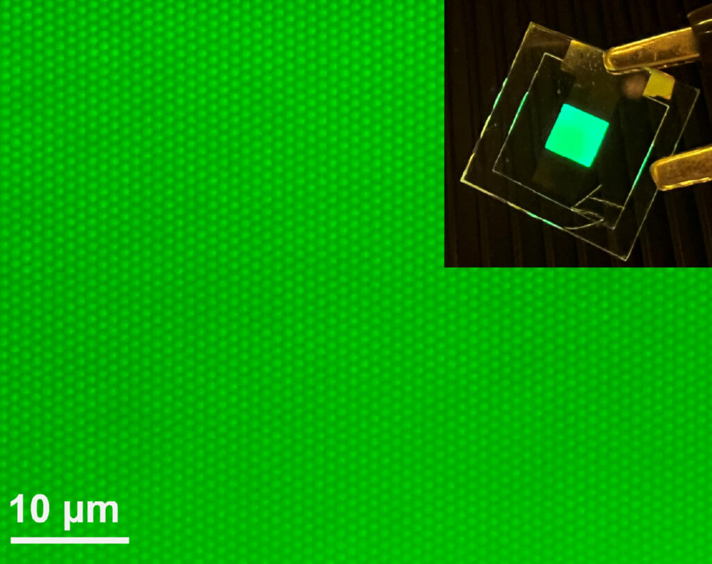
Micro-nano material and device prototyping
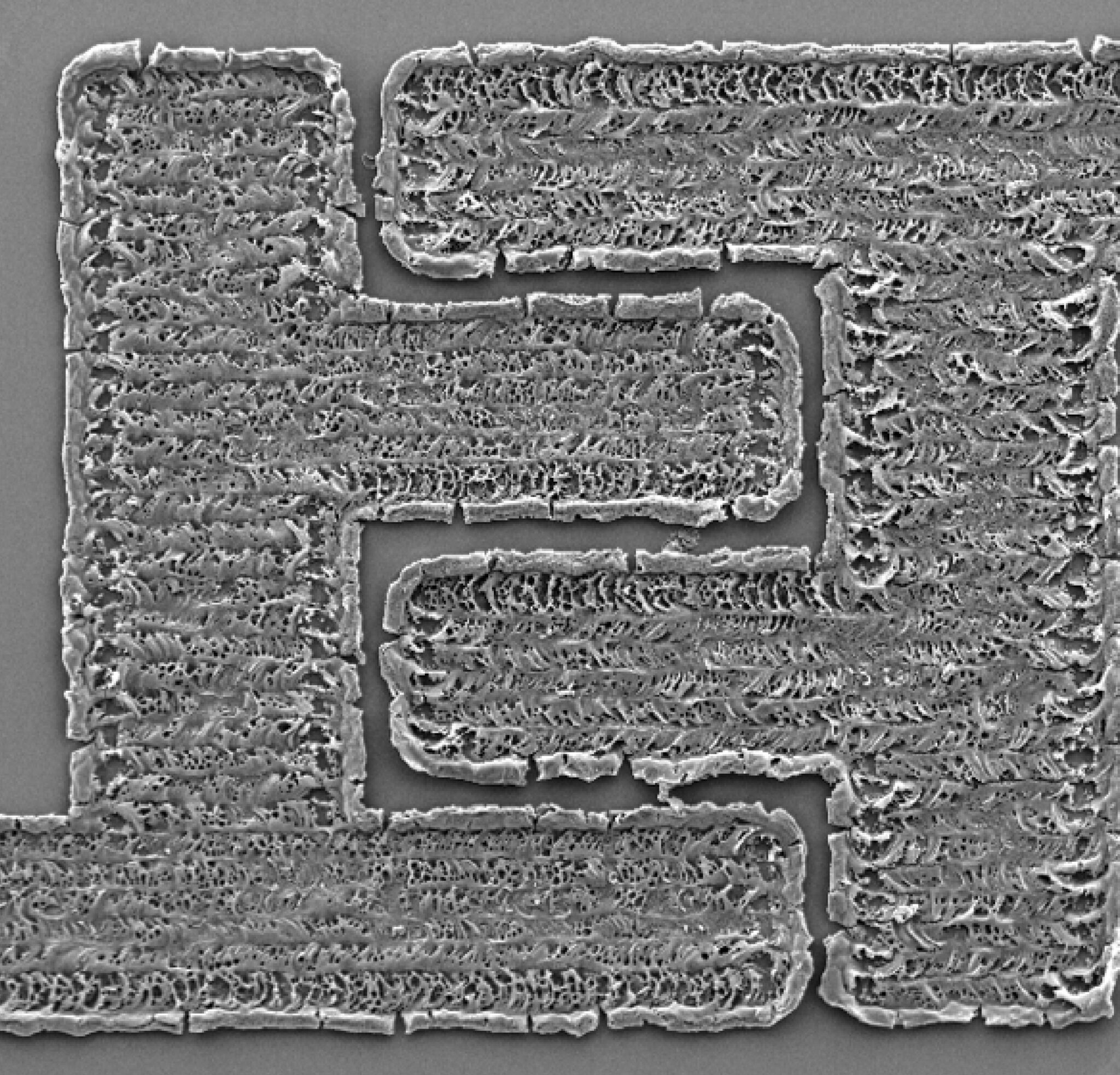
Suitable for high-resolution patterning of quantum dots, functional thin films, microelectrodes, and micro-nano optoelectronic device samples.
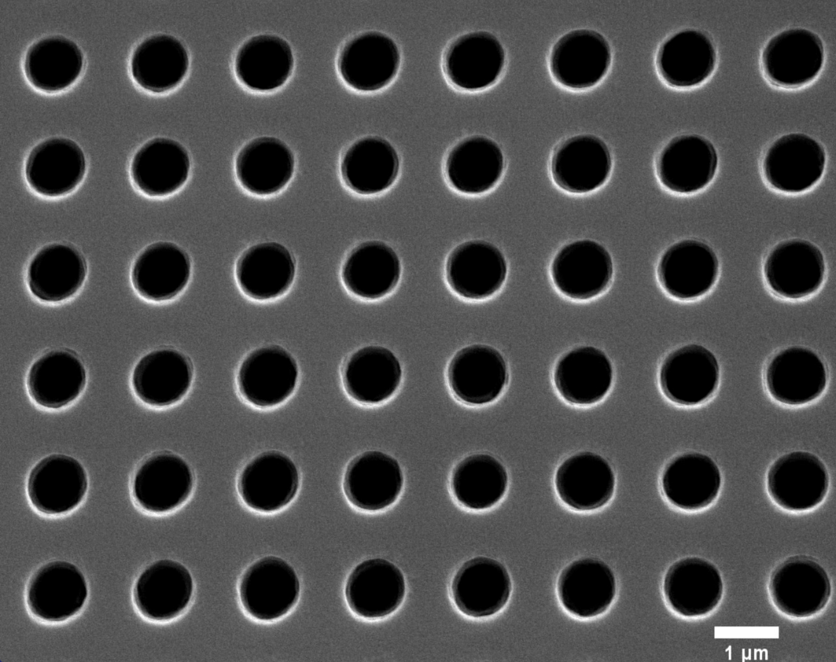
Micro-Optics and Diffractive Functional Structures
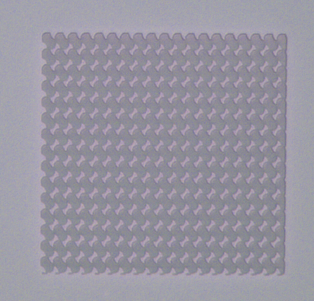
Suitable for high-precision fabrication of diffractive optical elements (DOE), periodic/aperiodic microstructures, functional surface textures, and micro-optical prototypes.
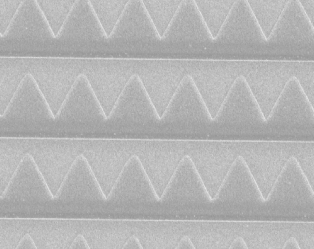
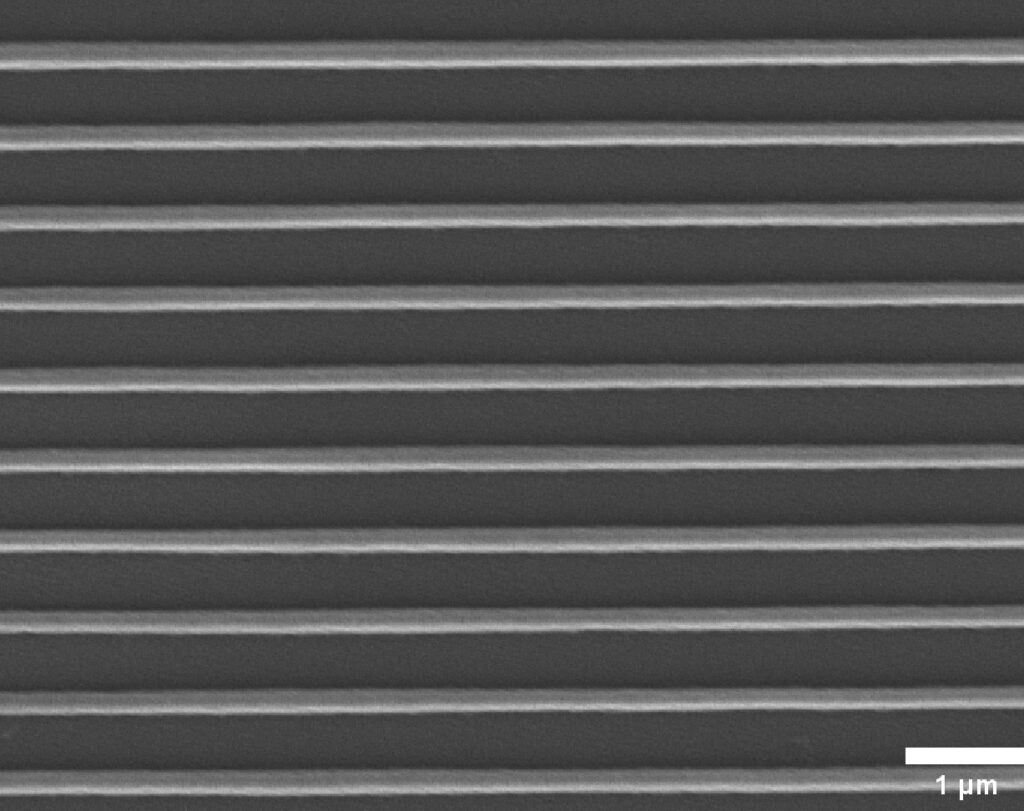
Designed for universities, research institutes, and corporate R&D departments, supporting rapid fabrication, parameter optimization, and experimental validation of micro-nano structure samples.
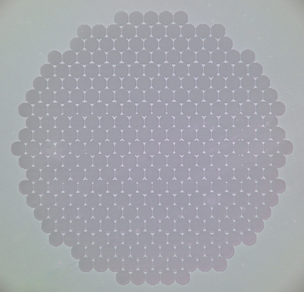
Exploring a New Era of Optics, Leading the Future of Technology.

Copyright © 2025 Astra Optics Limited