
In the journey toward the industrialization of 3D nanoprinting, two major challenges must be overcome: “printing fast” and “printing reliably.” Increasing manufacturing speed addresses production capacity, while ensuring manufacturing consistency directly determines yield.
In 2026, Professor Shi-Qi Chen’s team at The Chinese University of Hong Kong, in collaboration with researchers from ETH Zurich (Swiss Federal Institute of Technology Zurich), published a breakthrough study in Nature Communications. The team proposed a new closed-loop two-photon lithography system. Its most significant feature is that it can detect fabricated structures in real time during printing and automatically adjust printing parameters based on measurement results to correct deviations immediately.
With this capability, the team fabricated millimeter-scale optical components during a continuous 14-hour manufacturing process, achieving an overall dimensional error below 100 nanometers. This work demonstrates, for the first time, that two-photon lithography can achieve a true “print, inspect, and correct simultaneously” closed-loop manufacturing capability in long-duration and large-scale fabrication scenarios.
A Long-Overlooked Challenge: Instability of Printing Results
Two-photon lithography (TPL) is one of the most advanced 3D nanoprinting technologies currently available. Its principle is based on precisely focusing a femtosecond laser beam inside a photoresist. Only within the extremely small focal region is the light intensity sufficiently high to trigger material polymerization and solidification.
This “only the focal point is activated” characteristic allows TPL to sculpt nanoscale structures point-by-point in three-dimensional space with extremely high precision.
However, to apply this technology to large-scale manufacturing, one fundamental technical bottleneck must be overcome:
The printing results lack sufficient stability and repeatability.
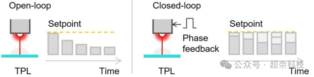
Almost all conventional TPL systems operate in an open-loop mode. The entire fabrication process uses a predefined set of parameters from beginning to end, without making any adjustments based on actual process conditions.
However, in real-world environments:
- Laser power gradually drifts;
- Ambient temperature fluctuates;
- Mechanical vibrations occur;
- Liquid photoresist itself may flow or change.
When printing small structures, these fluctuations may be negligible. However, once the process involves long-duration and large-scale fabrication, errors accumulate continuously over time. Eventually, these accumulated deviations can cause the entire device to fail.
Even more challenging is that traditional inspection methods are almost ineffective in this situation.
Post-process inspection cannot prevent problems in advance
Electron microscopy and atomic force microscopy (AFM) offer extremely high resolution, but they can only be used after printing is completed. Furthermore, they cannot operate directly inside the liquid printing environment. Once defects are discovered, it is already too late to correct them.
Conventional optical microscopy cannot resolve nanoscale details
Due to the optical diffraction limit, conventional optical microscopy cannot clearly resolve features below approximately 200 nanometers, nor can it provide three-dimensional structural information.
Therefore, most approaches in the industry still rely on repeated trial fabrication:
Strictly controlling parameters and environmental conditions, producing many samples, and waiting until a satisfactory one is obtained by chance.
This approach is not only time-consuming and expensive but also results in significant material waste.
Core Concept: Using the Same Laser Source for Both Printing and Inspection
The key innovation of Professor Chen’s team lies in using a specially designed laser system to perform both fabrication and measurement, thereby transforming the entire process into a closed-loop system.
The laser source is a dual-comb laser system, which can be understood as a system capable of simultaneously generating two complementary laser beams.
One beam is wavelength-converted and used for printing, triggering the solidification of the photoresist.
The other beam is dedicated to in-situ measurement of the forming structures, continuously acquiring real-time height and morphology information.
Because both beams originate from the same laser source and share the same time reference, they are naturally highly synchronized. This eliminates the need for additional complex stabilization systems and enables both high-speed operation and high-precision feedback.
During printing, the measurement beam continuously scans the working area and feeds the actual structural height information into a dynamic model.
The model compares the measured structure with the designed target. Once deviations are detected, it immediately adjusts:
- Laser power;
- Scanning speed;
- Exposure time;
bringing the structure back to the desired state.
Because solidification of the photoresist is irreversible, the system adopts a conservative strategy of “slightly underexpose first, avoid overexposure.”
Based on the prediction model, the process begins with approximately half of the required exposure dose. The system then dynamically adjusts exposure parameters according to real-time measurement results through additional exposure cycles, until the structure reaches the target height precisely.
Furthermore, whenever the fabrication position moves to a new location, the model updates itself using the latest measurement data, ensuring consistently accurate fabrication results.
Experimental Results: A Qualitative Leap in Long-term Manufacturing Stability
The team conducted a comparative experiment in which both an open-loop system and a closed-loop system were used to continuously fabricate the same type of microstructure arrays.
The results showed that:
The open-loop system began to exhibit significant deviations in structural height from the target value after only one hour of printing. By the tenth hour, the accumulated average error had exceeded one thousand nanometers.
In contrast, the closed-loop system maintained highly accurate structural dimensions throughout the entire fabrication process, with the average error remaining at only several tens of nanometers.
This improvement in stability was directly converted into performance advantages.
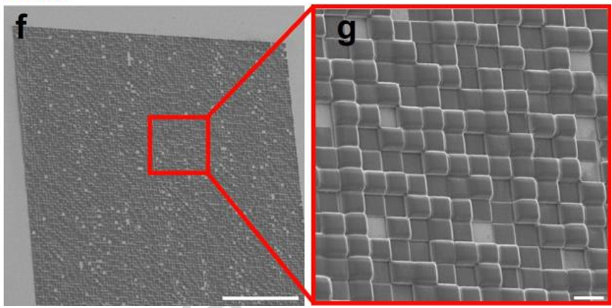
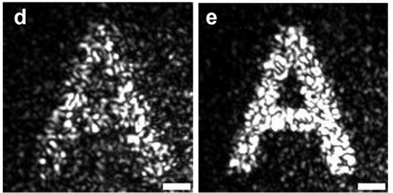
The team fabricated millimeter-scale diffractive optical elements and phase lenses.
For the diffractive optical elements:
- The structures fabricated by the closed-loop system produced projected patterns that were clear and sharp.
- The open-loop system produced significantly blurred patterns with more visible noise.
In lens performance testing, the closed-loop fabricated lenses also demonstrated substantially improved:
- Uniformity of focal points;
- Imaging quality;
- Optical performance consistency;
compared with lenses fabricated using the open-loop system.
In addition, the system shows excellent adaptability:
It can be applied to both:
- Transparent substrates;
- Opaque substrates.
Moreover, the entire system requires only one laser source to simultaneously perform printing and measurement, resulting in:
- A compact system architecture;
- Reduced complexity;
- Controllable cost.
“Increasing Speed” and “Improving Quality”: Two Technical Paths from the Same Research Team
This closed-loop system is not an isolated achievement. Rather, it represents an important part of Professor Chen’s team’s long-term research strategy toward achieving high-quality and high-throughput two-photon lithography (TPL).
Previously, the team introduced Line-scanning Temporal Focusing Two-photon Lithography (Line-TF TPL), which primarily focused on improving fabrication speed.
This technology transforms the femtosecond laser focus into programmable line-shaped patterns. Combined with continuous substrate scanning, it breaks the traditional intermittent printing mode of:
“stop, move, stop again”
and enables truly continuous, large-area 3D nanoprinting.
The newly developed closed-loop dual-comb laser system, however, focuses on manufacturing quality.
Rather than pursuing ultimate printing speed, it addresses the critical challenge of maintaining consistency during:
- Long-duration fabrication;
- Large-scale manufacturing.
It gives the printing process the ability to perform real-time self-correction.
Continuous fabrication solves the problem of:
“How to manufacture faster.”
Closed-loop error correction solves the problem of:
“How to manufacture reliably.”
When a system can simultaneously achieve:
- Continuous high-speed operation;
- Nanometer-scale consistency over long fabrication periods;
3D nanomanufacturing finally obtains the complete capability required for industrial-scale production.
Application Prospects
With significantly improved stability and repeatability, this closed-loop system is expected to play an important role in multiple advanced technology fields.
6G Communication Optical Components
Fabricating optical components with extremely high precision requirements while ensuring consistent performance across large-volume production.
Data Storage and 3D Display Technologies
Enabling long-term, stable fabrication of large-area, high-resolution structures, providing reliable manufacturing solutions for:
- High-density optical storage;
- Holographic displays.
Photonic Integration and Ultrafast Computing
Ensuring the yield and consistency of large-scale optical components for applications including:
- Photonic chip interconnects;
- Optical computing systems.
Precision Micro-optical Manufacturing
Enabling mass production of:
- Microlenses;
- Zone plates;
- Diffraction gratings;
- Other micro-optical components.
Transforming the previous situation of:
“Only producing qualified devices by trial and error”
into a manufacturing process that is:
“Stable, controllable, and repeatable.”
Note:
This article was prepared based on the preprint version of the research published in Nature Communications. The final officially published version may contain editorial revisions.
Reference:
Closed-loop High-precision Two-photon Lithography based on a Multiplexed Single-cavity Dual-comb Laser
Nature Communications