
In the development of modern optical technology, Diffractive Optical Elements (DOE) have gradually become a field of great interest. By utilizing the diffraction phenomenon of light, they manipulate optical waves with micrometer-scale or even nanometer-scale precision (such as metasurfaces), achieving many functions that traditional optical components cannot realize. For example, DOE can split a single laser beam into multiple beams, which is used for multi-channel signal transmission in optical communications [1]. Compared with traditional refractive and reflective optical elements, DOE has advantages such as flexible design, compact size, and light weight, and is widely used in optical communication, laser processing, optical measurement, imaging systems, and consumer electronics. This popular science article will briefly introduce the definition of DOE, common fabrication methods, and various practical applications.
Definition
Diffractive Optical Elements (DOE) are optical components that use the diffraction phenomenon of light to manipulate optical waves. Diffraction is the phenomenon in which light waves bend and interfere when encountering obstacles or apertures, and DOE precisely changes the propagation path and phase of light by designing and etching micro- or even nano-scale structures on its surface [3]. Unlike traditional optical components that manipulate light through refraction and reflection, DOE achieves more complex optical functions through diffraction effects.
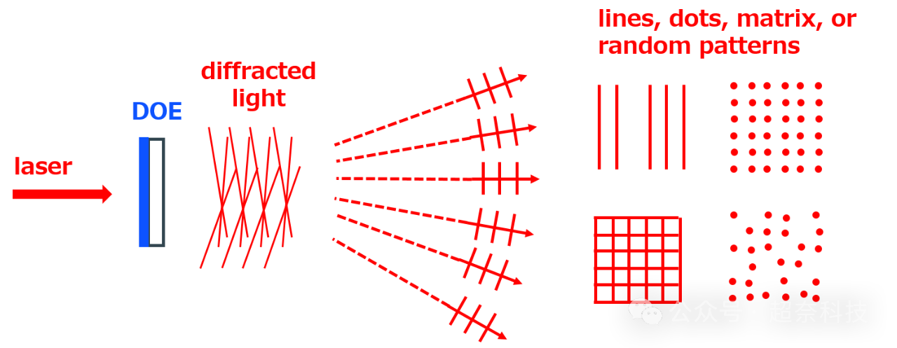
The basic principle of DOE involves the interference and diffraction of light. By designing specific patterns or microstructures, DOE can precisely change the optical path of transmitted light, thereby achieving control over the phase and amplitude of the light wave. These patterns are usually formed on the material surface by high-precision photolithography or electron beam lithography [4][5]. When light passes through these structures, diffraction and interference occur, thereby changing the propagation direction and intensity of the light. This method can not only realize the splitting, combining, and focusing of a single beam, but also generate complex optical patterns and holographic images [6].
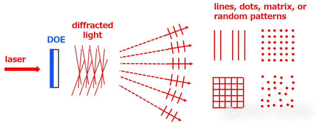
Schematic diagram of various patterns formed by diffraction and interference after light passes through DOE
The design and fabrication of DOE require precise mathematical modeling and high-precision processing technologies. By optimizing the geometric shape and arrangement of diffractive structures, a variety of complex optical functions can be realized. For example, by designing and fabricating periodic structures along the axial direction of optical fibers, selective reflection or transmission of specific wavelengths of light can be achieved, thereby realizing wavelength selection functions [7]. A typical example is the Distributed Bragg Reflector (DBR) based on multilayer media, which selectively reflects specific wavelengths of light waves by adjusting the thickness and refractive index of each layer [8]. In addition, non-periodic structures can also achieve broadband optical filtering functions. These characteristics enable DOE to play an important role in many high-precision and high-demand optical applications [9].
Fabrication Methods
In this article, we mainly introduce the fabrication aspect of DOE, which matches the processing technologies of Astra Optics. The fabrication of Diffractive Optical Elements (DOE) requires highly precise processing technologies to ensure micrometer- or even nanometer-scale structural accuracy. The following are several common fabrication methods, each with its own advantages and disadvantages [9–19]:
1. Photolithography
Photolithography uses photosensitive materials and photomasks to fabricate micro- or nano-scale structures through exposure and development processes. First, a layer of photoresist is coated on the substrate, then the pattern is transferred onto the photoresist through a photomask, and after development, etching, and removal of residual photoresist, the desired microstructure is finally obtained.
Advantages:
High resolution: capable of fabricating submicron-scale fine structures.
High production efficiency: suitable for large-scale production, especially widely used in the semiconductor industry.
Disadvantages:
High equipment cost: photolithography machines and mask fabrication equipment are expensive.
Complex process: requires multiple steps such as exposure, development, etching, and cleaning.
2. Electron Beam Lithography
Electron Beam Lithography (EBL) uses a focused electron beam to directly write patterns on the resist. It does not require a mask and can directly draw nanoscale fine patterns on the photoresist. Then, the pattern is transferred to the substrate through development and etching processes.
Advantages:
Ultra-high resolution: can reach nanometer-scale resolution.
Precise control: suitable for fabricating extremely complex and fine structures.
Disadvantages:
Slow speed: compared with photolithography, EBL has a slower writing speed and is not suitable for large-scale production.
High cost: equipment is expensive and operation is complex.
3. Laser Direct Writing
Laser Direct Writing uses a laser beam to directly etch the material surface to form the required pattern. This method has high flexibility, allowing rapid design changes, and is suitable for prototyping and small-batch production.
Advantages:
High flexibility: allows rapid design changes, suitable for prototyping and small-batch production.
No mask required: avoids the cost and time of mask fabrication.
Disadvantages:
Limited resolution: lower resolution compared to electron beam lithography.
Moderate speed: slower than photolithography but faster than EBL.
4. Nanoimprint Lithography
Nanoimprint Lithography (NIL) uses a mold to imprint micro- and nanostructures onto the material surface. First, a high-precision mold is fabricated, then pressure and heat are applied to transfer the pattern from the mold onto the material surface.
Advantages:
High resolution: can reach nanometer-scale resolution.
Low cost: relatively lower equipment and operating cost compared to other high-resolution techniques.
Disadvantages:
Complex mold fabrication: requires high-cost and precise processes.
Limited applicability: suitable for large-scale production but not for rapid prototyping.
5. Ion Beam Etching
Ion Beam Etching (IBE) uses high-energy ion beams to etch the material surface. It allows precise control of etching depth and pattern and is applicable to various materials, including metals and semiconductors.
Advantages:
High precision: suitable for fabricating high-precision and high aspect ratio structures.
Material versatility: can process a variety of materials, including hard materials.
Disadvantages:
High cost: equipment and operation are expensive.
Slow speed: not suitable for large-scale production.
Applications
Diffractive Optical Elements (DOE) are widely used in multiple fields. The following are five representative applications:
1. Optical Communication
In optical fiber communication systems, DOE is used to split and combine beams to improve communication efficiency. DOE can divide a single laser beam into multiple beams to achieve multi-channel signal transmission. This method increases system capacity and data transmission rates. In addition, DOE can be used in wavelength division multiplexing (WDM) systems to selectively reflect or transmit specific wavelengths for signal multiplexing and demultiplexing.
Examples:
NKT Photonics: provides DOE products for optical communication systems [20]
OptoSigma: produces diffractive optical elements for optical communication [21]
2. Laser Processing
DOE is used in laser processing for beam shaping and splitting to improve processing precision and efficiency. For example, in laser cutting and welding, DOE can split a single beam into multiple smaller beams to improve uniformity and speed. It can also be used in laser micromachining to focus the beam into extremely small spots for high-precision material removal.
Examples:
Coherent Inc.: provides DOE products for laser processing [22]
Jenoptik: produces DOE for industrial laser processing [23]
3. Optical Measurement
In optical measurement technologies, DOE improves accuracy and resolution. In applications such as Optical Coherence Tomography (OCT) and interferometry, DOE is used for beam shaping and splitting to enhance imaging clarity and measurement precision.
Examples:
Thorlabs: provides DOE products for optical measurement [24]
Zygo Corporation: produces high-precision DOE [25]
4. Imaging Systems
In imaging systems such as microscopes and astronomical telescopes, DOE is used to correct aberrations and improve image quality. By controlling different wavelengths, DOE can reduce chromatic and optical aberrations. It is also used in multispectral and hyperspectral imaging systems.
Examples:
Olympus: provides DOE for microscopy systems [26]
Zeiss: produces DOE for high-end imaging systems [27]
5. Consumer Electronics
In VR and AR devices, DOE is used to generate holographic images and light-field displays, improving visual experience. It is also used in optical sensors to enhance sensitivity and precision.
Examples:
Magic Leap: AR devices using DOE [28]
Microsoft HoloLens: AR headset integrating DOE [29]
Summary
As a new type of optical component, Diffractive Optical Elements (DOE) achieve precise control of light waves through microstructure design and fabrication. This article introduced their definition, fabrication methods, and representative applications. From optical communication to laser processing, optical measurement, and imaging systems, DOE demonstrates broad application prospects. With the advancement of fabrication technologies and increasing demand, DOE will play an increasingly important role in the future of optics.
Additional Section (Femtosecond Laser Part)
Figure (a) shows traditional two-photon excitation. In this technique, an ultrashort pulse is spatially focused to a single point, generating high peak intensity at that point. However, when this pulse passes through certain samples (such as photoresist), its duration remains nearly unchanged. If the intensity is sufficiently high, polymerization may occur above and below the focal point.
Figure (b) shows the effect of temporal focusing on pulse duration Δt and spatial spot size. First, the illuminated area near the focal plane is several orders of magnitude larger than that of spatial focusing, which is referred to as plane excitation. Second, as the pulse propagates in the sample, its temporal width broadens. Only at the focal plane does it reach its peak intensity. Before and after the focal plane, the pulse is stretched, preventing two-photon excitation and greatly improving axial resolution.
Technical Implementation
Initially, temporal focusing was implemented using a diffraction grating to separate the spectrum of femtosecond laser pulses, followed by a 4-f system to conjugate the grating with the back focal plane of the objective lens, projecting the grating onto the sample plane. However, this method used a static grating and could not dynamically switch patterns, limiting it to imaging applications.
Later, the research team led by Professor Chen Shiqi at The Chinese University of Hong Kong introduced a Digital Micro-mirror Device (DMD) into the system. Since the DMD itself acts as a two-dimensional grating, it introduces dispersion similar to a conventional grating. More importantly, it is dynamically programmable and can project various patterns.
Challenges
The main challenges include femtosecond laser stability and strict environmental control. High-energy laser operation requires precise conditions, as even slight deviations may cause errors or failure in fabrication.
To address these issues, the team employed high-precision positioning systems, controlled laboratory environments, and optimized post-processing procedures.
Another challenge is dispersion control, which directly affects resolution. Through extensive experiments and simulations, the system was optimized and successfully implemented.
This work was published in Science in 2019 and received wide recognition.
Conclusion
Spatiotemporal focusing of femtosecond lasers originated in two-photon imaging and has gradually been applied to 3D nanofabrication. Compared with traditional point excitation, it enables plane excitation, significantly improving fabrication speed without sacrificing resolution.
With its flexibility and efficiency, this technology shows great promise for future applications.
References
[1] Zhu, Guanghao, et al. “Simultaneous spatial and temporal focusing of femtosecond pulses.” Optics express 13.6 (2005): 2153-2159.
[2] Oron, Dan, Eran Tal, and Yaron Silberberg. “Scanningless depth-resolved microscopy.” Optics express 13.5 (2005): 1468-1476.
[3] S.K. Saha, D. Wang, V.H. Nguyen, Y. Chang, J.S. Oakdale, S. Chen, “Scalable Submicrometer Additive Manufacturing,” Science, Vol. 366, No. 6461, pp. 105-109, 2019.
[4] Sugioka K, Cheng Y. Ultrafast lasers—reliable tools for advanced materials processing[J]. Light: Science & Applications, 2014, 3(4): e149-e149.
[5] Gansel, Justyna K., et al. “Gold helix photonic metamaterial as broadband circular polarizer.” science 325.5947 (2009): 1513-1515.
[6] Watanabe, Wataru, et al. “Wavelength division with three-dimensional couplers fabricated by filamentation of femtosecond laser pulses.” Optics letters 28.24 (2003): 2491-2493.
[7] Skryabin, N. N., et al. “Two-qubit quantum photonic processor manufactured by femtosecond laser writing.” Applied Physics Letters 122.12 (2023).
[8] Piacentini, Simone, et al. “Advanced photonic and optofluidic devices fabricated in glass via femtosecond laser micromachining.” Optical Materials Express 12.10 (2022): 3930-3945.
[9] Lyu W, An J, Lin Y, et al. Fabrication and applications of heterostructure materials for broadband ultrafast photonics[J]. Advanced Optical Materials, 2023, 11(12): 2300124.
[10] Liu H, Lin W, Hong M. Hybrid laser precision engineering of transparent hard materials: challenges, solutions and applications[J]. Light: Science & Applications, 2021, 10(1): 162.
[11] Han, Fei, et al. “Three-dimensional nanofabrication via ultrafast laser patterning and kinetically regulated material assembly.” Science 378.6626 (2022): 1325-1331.